Data Line Analysis Dialog Parameters
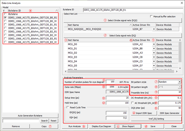
Figure 1.
- Select Strobe signal nets: Strobe signal net for analysis can be selected over Select Net dialog.
- Select Data signal nets: Corresponding data byte nets for analysis can be selected over Select Net dialog.
- Net Name: all selected net names are listed.
- Active Driver: you can specify the active driver pin among the connected pin to this net. The other pins will be assigned as receiver pin(s) automatically. For write cycle analysis select CPU component as an active driver pin.
- Device Models: For the selected active driver, actual driver model can be
selectable among many different models in IBIS or Linear device model types.
You can use one of available models considering the output impedance,
driving capability measured by output current level and operating
frequencies. These driver’s characteristics lead huge impact on the
simulated waveforms.
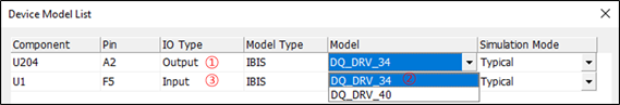
Figure 2. - Number of random pulses for eye diagram: Means the number of random pulses excited to the simulating net during the eye diagram analysis.
- Bit pattern style: Select the numerical method among random, ABS (Artificial Bit Stream) and PRBS (Pseudo Random Bit Stream) for generating the bit sequences. ABS (Artificial Bit Stream) is a method designed to provide a large pattern of bits to show worst case signal transmission quality of the net that would quickly converge the eye diagram. PRBS (Pseudo Random Bit Stream) is the mostly common method deemed as an industry standard.
- Bit pattern length: if bit pattern style is ABS or PRBS, choose the bit pattern length.
- Preamble time: Simulation start after this time to wait until status of internal circuit becomes stable.
- Data rate: Shows DDR operating speed.
- Setup time: Shows required setup time.
- Hold time: Shows required hold time.
- DC threshold: Shows threshold voltage value for hold time measurement.
- AC threshold: Shows threshold voltage value for setup time measurement.
- DQS jitter: Enter system DDR data bus jitter value.
- Import: By clicking the Import tab, you can choose required DDR
operating speed from pre-defined table. Then the contents field
10~15 will be filled with pre-defined value from JEDEC
specification. It supports up to the specifications of DDR2,3,4.
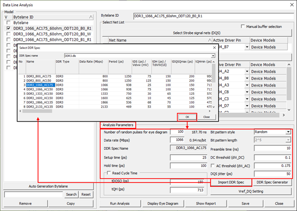
Figure 3. - Run Analysis: Simulation starts.
- Show Report: The analysis results can be listed in a table form by
clicking the Show Report tab. They can be also shown in MS
Excel.
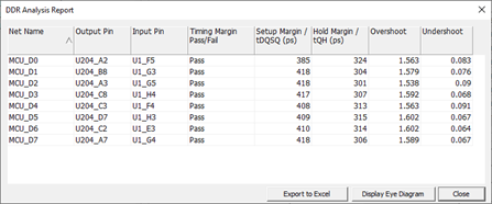
Figure 4. - Save: Save menu saves the file in Signal_Integrity/Waveform directory under the PCB design job folder. The model name plus .spe is used for the file name. The saved eye diagram waveform data can be read into the waveform viewer alone or together with other eye diagram waveform data.
- Model Name: Model name of the simulated and saved nets are listed.
- Copy: This menu enables the selected net(s) to be registered at Select Net region for analysis.
- Import: By clicking the Import tab, you can choose required DDR
operating speed from pre-defined table. Then the contents field
10~15 will be filled with pre-defined value from JEDEC
specification. It supports up to the specifications of DDR2,3,4.