IC Visual mark
Check the validity of design for IC visual mark in footprint.
If the SMD type components have a small pin pitch, it needs an IC visual mark so that machinery can detect the component location and direction.
The IC Visual Mark dialog contains the following sections:
- Visual Mark Definition: Define the target component and IC visual mark
specification in components.
- Component Definition
- Component Group: Define the component group that should have an IC visual mark. Select a component group from the list.
- Select Components with Pin Information: Define fine pitch
components with pin pitch and the number of pins.
- Maximum Pin Pitch: Set the component maximum pin pitch.
- Minimum Number of Pins: Set the component minimum number of pins.
- IC Visual Mark Definition: For components selected, set the
specification of IC visual mark.
- Component Group: If IC visual mark is defined with component, define it from the component group list. In many cases, IC visual marks are defined with the combination of pads and solder resist. In those cases, use the below method to define IC visual mark with mark size and pad size.
- Mark Size (MS): Set the mark size ranges using range input tool.
- Pad Size (PS): Set the pad size ranges using range input tool.
- Mark Location Area Definition: Set the IC visual mark location area
from the component outline
- Outer Size (OS): Define the outer size from component outline.
- Inner Size (IS): Define the inner size from component
outline.
Figure 1. 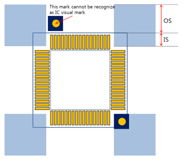
- Component Definition
- Visual Mark Checking
- Diagonal Existence Check: Check if IC visual marks are diagonally
placed. If the specified component doesn’t have a diagonally placed
visual mark, it results in a fail.
- Number of IC Visual Mark in Corner: In diagonal existence checking, the number of marks in each corner should be matching with the given number.
- Minimum Number of Marks: Check the total number of marks in a component.
- Copper Existence Checking on Mark Area: Check If the IC visual mark is overlapping with the copper-pour.
- Check for all layer: If IC visual mark is placed on a certain layer,
even on the other layer, it cannot to be overlapped with copper-pour
in the other area.
Figure 2. 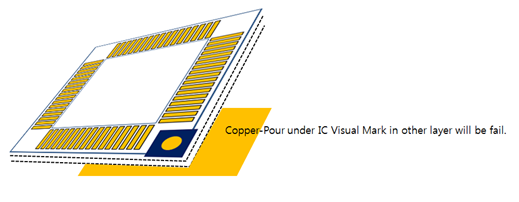
- Overlapping Check with Silkscreen: Check if IC visual marks overlapping with another silkscreen object.
- Diagonal Existence Check: Check if IC visual marks are diagonally
placed. If the specified component doesn’t have a diagonally placed
visual mark, it results in a fail.