BGA
Check the rules for BGA component clearance and via placements near pins.
The BGA dialog contains the following sections:
- BGA Component Definition
- BGA Component Group: Select the BGA component group from the predefined component group list.
- Laser Via Definition: If laser vias are used on PCB design, it is able to
check the clearance with certain value.
- Maximum Hole Size: Can define the via with having hole size.
- Via Padstack Selection: Can define the via with using name.
- Padstack String: Can define the via with using string filter.
- Import(.txt): Apply Filter Type based on the characters
entered in the .txt file.
- Apply as a prefix when (|F|) ABC is entered in the .txt file.
- Apply as a mid-string when ABC is entered in the .txt file.
- Apply as a suffix when ABC(|P|) is entered in the .txt file.
- Export(.txt): Export the characters registered in the String Item in .txt file format.
- Import(.txt): Apply Filter Type based on the characters
entered in the .txt file.
- Via Location Checking: Check the via location. Depending on the options, if
the via is placed among the center of the pins or at the same location, it
passes.
Figure 1. 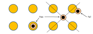
- Pass for the center of 4BGA Pins.
- Tolerance: Even if a Via Location design violation occurs, if it is within the inputted tolerance value, it is regarded as a pass.
- Pass for the same BGA Pin’s Location.
- Tolerance: Even if a Via Location design violation occurs, if it is within the inputted tolerance value, it is regarded as a pass.
- Pass for the center of 4BGA Pins.
- Clearance Checking in BGA: Among defined BGA components, pick the BGA
components with certain pin pitches and specify special clearances for
different items. Set the pin pitch and double-click the Check
Option column. In the dialog, set various clearance options
and click OK to save them.
In the column, selected clearances option numbers will be displayed.
Figure 2. 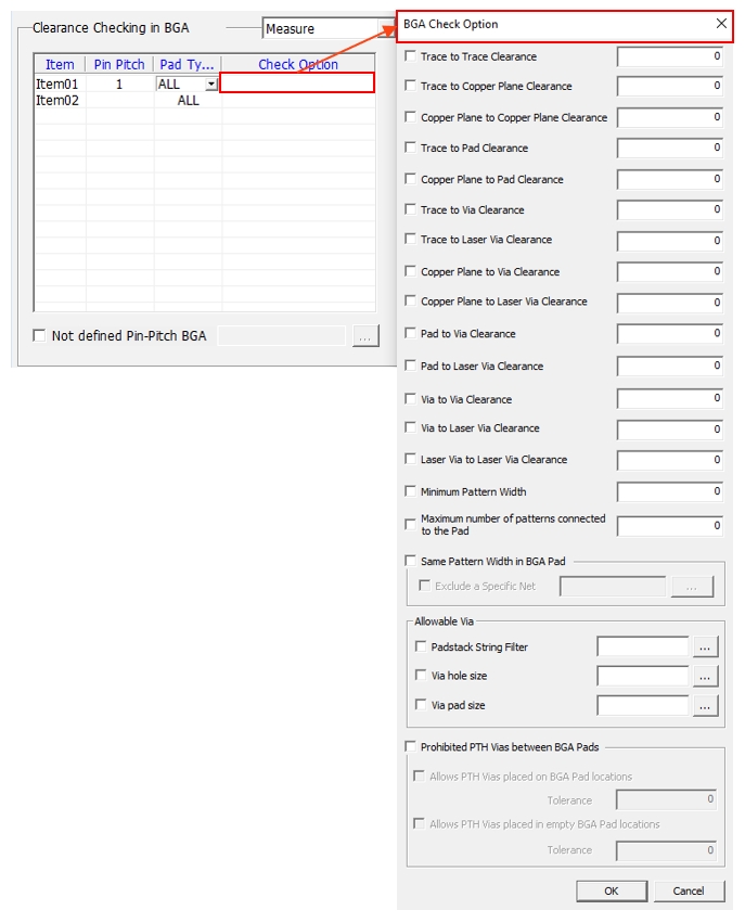
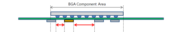
- Clearance between Components under BGA Area on BGA’s Reverse Side: For
components that are placed on the reverse side of BGA components and under
the BGA component area, use PollEx DFM to check the
clearance among them. Select the component group1, component group2, and set
the clearance values to complete rule.
Figure 3.