DIP Annular Ring
Check the DIP type pad size ratio against the hole size.
Narrow distance from the outer hole to the pad edge may result in a shortage of solder or an electrical spark while operating.
The DIP Annular Ring dialog contains the following
sections:
- Component DIP Annual Ring Size Checking: Check DIP type pads annual ring
size.
- Layer Definition: Select the layer.
- Target Layer Component's Placed Layer: Select the pin
location layer.
- All
- Top
- Bottom
- Target Layer: Select the target layer.
- Top
- Bottom
- Inner
- Target Layer Component's Placed Layer: Select the pin
location layer.
- Checking Table: To check the annual ring size, complete each row.
- Item: Set item name.
- Comp Group: Double-click the column, after launching the component group selection dialog box, select the target component group.
- Target: Select the target annular ring as either Pad or Solder Mask.
- Hole Type: Select the All or DIP Type Hole(PTH) or DIP Type Slot Hole(PTH).
- Check Type: To check Annual Ring size, use minimum annual ring size or the pad ratio to hole. After using Hole/Pad Ratio (%), the unit will be a percentage (%).
- Default Value: Depending on the Check Type, set the value.
- Inner Layer Value: Set the Annular Ring value for the inner layer Pad.
- Opposite Side Value: Set the Annular Ring value for the pad that is placed on the opposite side of the component.
- Pad Existence: Check missing pads on all layers of DIP-type holes.
- Not Defined Component Group: For the components that are undefined, set another checking rule for them similar to the checking table.
- Exclude Pins, having Specified Hole Size: Among specified components, exclude checking for component pins that have a specified hole-size range. Use size range input tools.
- Exclude Checking for NC Pin: This is a void-checking option for NC (Non-Connection) pins.
- Layer Definition: Select the layer.
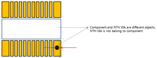
- NTH Via and Overlapping Pad’s Size Checking: If SMD components pad and
non-through holes are overlapped, gap between hole and pad should be
reserved.
Figure 1. 
- Target Component Group: Select the target component group from the list.
- Minimum Gap between Via hole and Pad: Set the minimum distance value between component pad and NTH Via.
- Non-functional Inner layer Pads: Verification of presence of non-functional
pad (Pad not connected to pattern or plane in inner layer) in inner layer.
If non-functional Pad exists, it is fail.
- Target Component Group: Select the target component group from the list.
- Exclude checking for specific Padstacks: Through String Filter,
specific Padstacks are excluded from verification.
- Import(.txt): Apply Filter Type based on the characters
entered in the .txt file.
- Apply as a prefix when (|F|) ABC is entered in the .txt file.
- Apply as a mid-string when ABC is entered in the .txt file.
- Apply as a suffix when ABC(|P|) is entered in the .txt file.
- Export(.txt): Export the characters registered in the String Item in .txt file format.
- Import(.txt): Apply Filter Type based on the characters
entered in the .txt file.