Router Machine JIG Generator Tutorial
After the SMD process, it goes through the router process that separates the unit of the panel PCB in the array.
At this stage, the router JIG is used to fix the panel PCB and suck the dust generated during the router process. Router-Machine JIG Generator provides to quickly generate design drawing for manufacturing JIG using PCB design data and panel PCB Gerber of array board.
-
Import Gerber data.
-
In the Import from Gerber (RS-274D/RS-274X)
dialog, click
 .
.
-
In the Import from Gerber (RS-274D/RS-274X)
dialog, click
-
Create Base Line.
-
For Select Gerber Layer, select Top-Metal.phd to
recognize the PCB outline and Bridge.
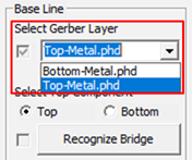
Figure 1. -
For Select Top Component, select Top.
Select Top because the top surface between the PCB design data and the manufacturing process may be different.
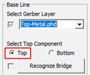
Figure 2. -
Click Recognize Bridge.
The line corresponding to the bridge is automatically searched. The recognized line of the bridge is displayed in white, and the vacuum hole is in red.
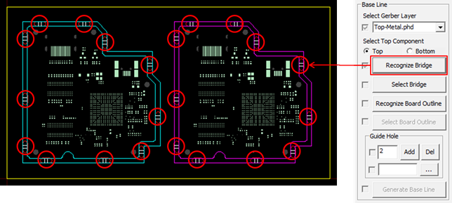
Figure 3. -
Click Recognize Board Outline.
The board outline is automatically recognized from the Gerber data.
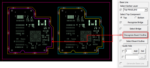
Figure 4. -
Click Select Unit PCB Outline.
The selected unit PCB outline is highlighted in red and is the basis for creating the base line.
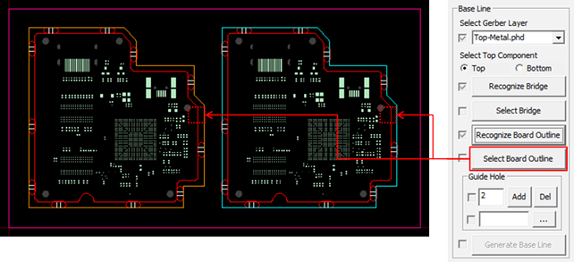
Figure 5. -
Repeat steps 5.f - 5.g until all guide holes in the PCB design are
selected.
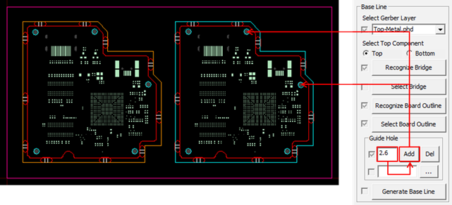
Figure 6. -
Click Generate Base Line.
The generated base line is displayed in green.
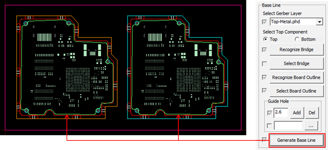
Figure 7.
-
For Select Gerber Layer, select Top-Metal.phd to
recognize the PCB outline and Bridge.
-
Click Generate JIG Size.
The outline of the router JIG is generated and is displayed in blue.
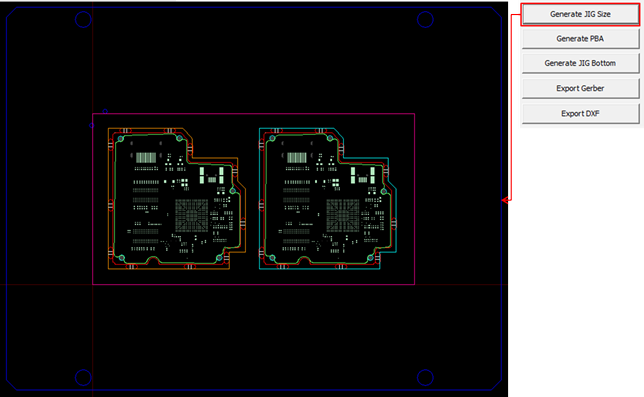
Figure 8. -
Click Generate PBA.
A processing line for panel PCB mounting on the router JIG which is generated and is displayed in yellow.
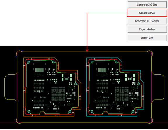
Figure 9. -
Click Generate JIG Bottom.
The bottom line of the router JIG is generated and is displayed in gray.
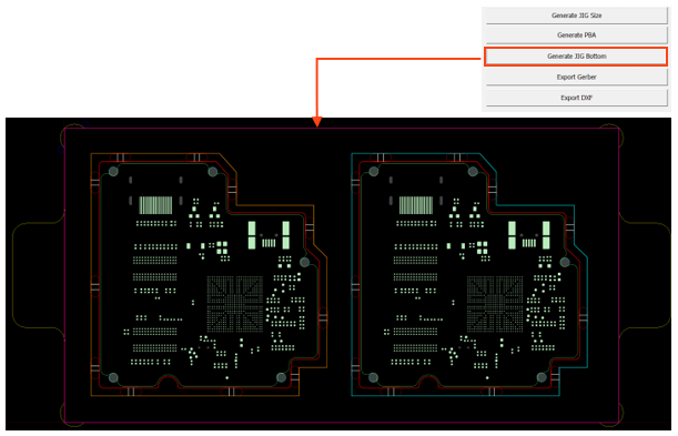
Figure 10. -
Export JIG Data.
-
Specify the path to save the data and click OK.
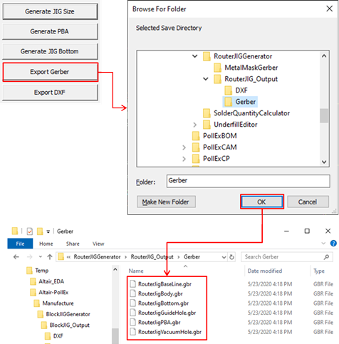
Figure 11. -
Specify the path to save the data and click
Save.
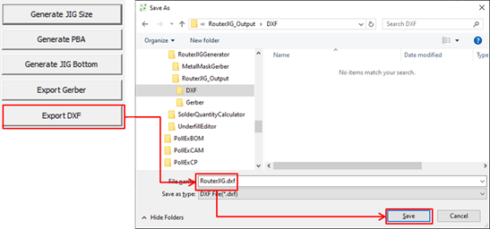
Figure 12.
-
Specify the path to save the data and click OK.