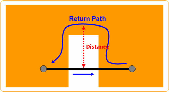
One of the ways to make high speed signals stable is by making a return path shorter.
If there is enough ground structure above and/or below the signal propagation path,
the return path usually follows the signal path in high speed design. If ground
patterns are cut by other structures or voids, return paths must go around such
voids so the return path lengths become longer than the desired length. This item
calculates the shortest signal return path along ground path. The shortest signal
return path may become several times longer than signal path. This item checks for
the ratio between the shortest return path length and signal length on
board.
Item: Input item name.
Net: Select a target Net from the Net Class list.
Reference: Select a Ground Net from the Net Class list to search for the
Return Path.
Pass/Fail Criteria: Define the value (Ratio or Distance) to detect the fail
of Return Path and Signal.
Check ratio: Check ratio between net length and return current path.
Check distance: Check maximum allowable detour distance of return
path. Figure 1.
Consideration: Addition factors for Return Path search.
Select Start Component in case of Branch net: When searching Return Path of
multiple pin (more than 2 pins) net, a start component must be defined.
Return paths are searched from the start component to all other components
or pins.
Except Component Group: Certain types of components or pins can be excluded
from searching return path. (For example, Test Points)
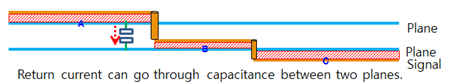
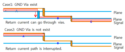
Flow current along via location: To search for the shortest return path one
multiple ground layers connected by via. When it is not checked, return path
is searched on a superimposed ground layer.
Not checked: The return current always goes through capacitance
between two planes regardless of via existence. Figure 2.
Check: The return current can go through only if there is stitching
via. Figure 3.
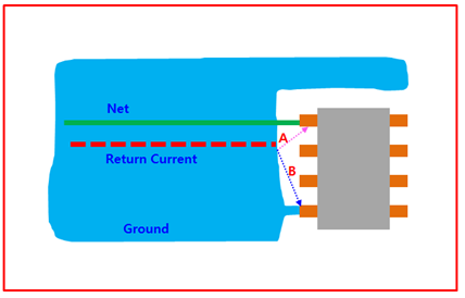
Ignore return path for near area to pin: Complete the return path search to
the ground plane edge.
Will not check pin area: Enter a radius of circular region around
pins to be excluded for the rule check.
Return path to pin: Select the way to complete the return path
search.
Consider Return Path from GND Pin to GND Pin: Complete the return
path search to the ground pins that are closest to the signal pins.
(Fig. below, path ‘B’)
Force make return path to pin: Force return path to connect to
directly to GND pins as shown in Fig. below. (Fig. below, path
‘A’) Figure 4. Return path connection compensation
The signal propagates between the signal trace and the reference plane and it acts
like a loop antenna. The electrical field strength of loop antenna is: Figure 5.
The electrical field strength is proportional to loop size, so it is very important
to reduce loop size of circuit in order to reduce EMI noise.