Copper Cross Over Detect
When a current flows on a signal trace, there is always a return loop. If some current goes out to somewhere, it will always come back to source. The path of returning current is Return Path. Return path is formed differently depends on frequency. At low frequencies, the current follows the path of least resistance. At high frequencies, current follows the path of least inductance and it stays tightly bunched near signal trace.
Return path is the shortest when signal trace is tightly shielded by solid ground plane below or by coplanar ground. However, any discontinuities, such as slots, gaps, holes and split planes, along the shortest return path makes the current to go around the discontinuities.
At high frequency, longer return path leads to an unexpected ground/power bounce and increases a possibility of EMI.
- Net Group: High speed signal net.
- Plane Net: Power and Ground net group to be used as return path structure.
- Check Layer: Plane layer on which return path will flow.
- All: All layers.
- L1 Layer: check one layer above and below.
- L2 Layer: check two layers above and below.
- Stitching Component: A stitching component provides a path for return
current to flow back to its source when the critical net crosses over the
plane split.
- Max Distance: The allowable maximum distance between cross over
point to stitching component.
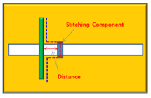
Figure 1.
- Max Distance: The allowable maximum distance between cross over
point to stitching component.
- Escape Area: Area close to pins or vias of target signal net can be excluded
for checking because there are holes on ground plane near pins or vias.
- Pin Escape: Enter a radius of circular region around pins to be excluded for the rule check.
- Via Escape: Enter a radius of circular region around vias to be excluded for the rule check.
- Allowable Detour Length: Enter maximum allowable signal return path
detour length when the signal crosses over the void area.
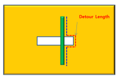
Figure 2.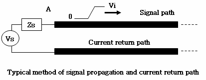
Figure 3.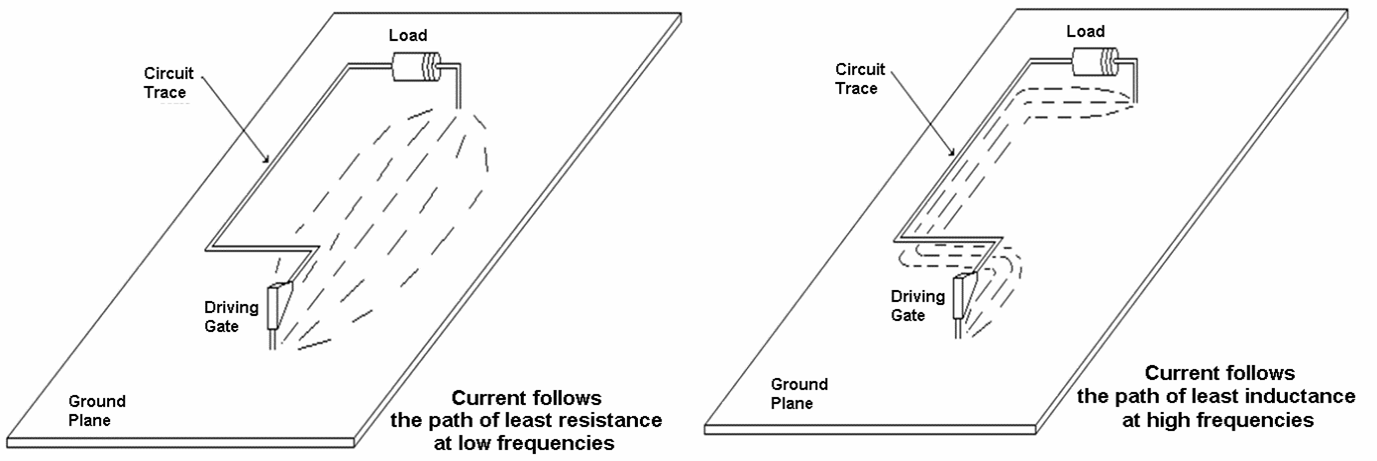
Figure 4.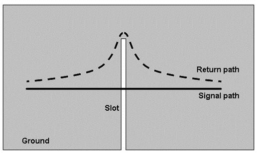
Figure 5.
- Impedance mismatch by copper discontinuity.
- Signal return path.
- Ground shield.