Approach GND VIA (Stitching Via)
This item checks whether high speed signal vias have their ground vias as shielding within a certain region.
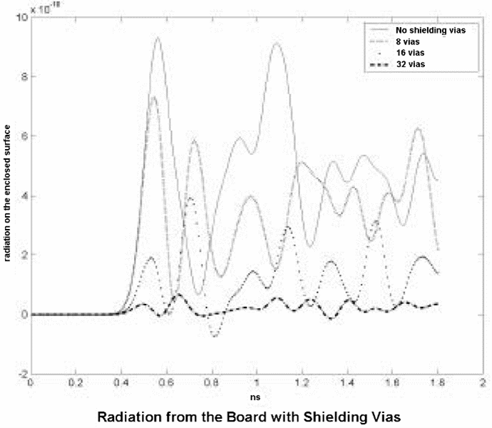
When there is an EMI problem, a first aid is shielding target traces with ground pattern. And as the increase of frequency, via also can be an element causing EMI trouble. Designers should reduce the trouble by placing ground vias near the target EMI source via. Depending on the product, consider how many ground vias should be used. Basically, the effect of two vias is the same as trace shielding. To make it more robust, placing four ground vias around a signal via is recommended.
In general, a signal that flows in a through-hole via does not cause much trouble. However, in high frequency, within via region, a phase shift may occur. To stabilize high speed signal, ground shielding becomes necessary. But a perfect via shielding is impossible. Instead of via shielding, it is better to place ground vias close to a signal via location.
Depending on products and design requirements, a number of necessary ground vias may vary. Normally the effect of two vias is the same as trace shielding. To achieve a more robust shielding effect, placing four ground vias around a signal via is recommended.
- Check Type: Determines measuring method.
- Shape: Measure edge to edge distance
- Position: Measure center to center distance
- Item: Input item name. This is written in the report for reference.
- Reference Plane: Select Power/analog ground Net Group.
- Net: Select High Speed Signal Net Group.
- Pin Escape: Enter a radius of circular region around pins to be excluded for the rule check.
- Distance: Distance from signal via within which shielding ground vias are supposed to be located.
- Min via Count: Number of shielding ground vias required within the distance.
- Component Keep IN/OUT: You can define the test region. For example, you can
test inside or outside the breakout region of CPU with different test
values. Double-click the blank field. The Component Keep in/out
Setup dialog displays.
- Component Group: Select the required component group used for defining the test region.
- Range (COC+distance): Enter the distance value to define breakout range. The COC (Component Overlap Check) plus this distance value is considered the test range.
- Region: Define the required test region.
IN: Test inside of the breakout region of target component.
OUT: Test outside of the breakout region of target component.
-
- Target Layer: Select the required test layer.
- All Layer: Test all layers.
- Component Place Layer: Test only component placement layer.
- Different Rule Setup in Special Region: Assign additional test
region for breakout region testing.
- Extended Region from COC: Enter the distance value to define additional range. The COC (Component Overlap Check) plus this distance value is considered the additional test range.
- Allowable Values: Assign additional allowable test value for
this additional region.
- Value: Add additional allowable value.
- Range: Add additional allowable range.
- Deviation: Add additional allowable value with deviation using this option.
- Deviation (%): Add additional allowable value with deviation (%)
- Target Layer: Select the required test layer.
- Stitching Component: A stitching component should be existing when critical net changes the reference planes. If the two planes are at the same potential, you only need to connect them together with a Via at the place where the critical net penetrates. But if the potential of two planes are different, vias would not work, so the capacitor would connect between the ground plane and power plane and must be located adjacent to where the critical nets change reference planes. Using this option, you can use Stitching component. Upon selecting this option and assigning stitching components, the DFE considers this stitching component as one stitching Via.