In this step, you will complete operational steps of the thermal analysis
tool.
Before you begin, download, uncompress, and save the sample
PCB design file, PollEx_PCB_Sample_r<revision
number>.pdbb, to a job folder you will use for this
tutorial.
Additionally, this tutorial is intended to demonstrate the process of
Thermal Analysis. The Thermal Engine is updated regularly, and as a result, the
Thermal Analysis result may vary slightly with each update.
This sample PCB design file is provided with PollEx Thermal.
PollEx Thermal is a board-level finite element thermal
analysis program.
Create Project
In this step, you will load the PCB design and create a new project.
Click File > Open.
Open the
PollEx_PCB_Sample_r<revision_number>.pdbb
file from
C:\ProgramData\altair\PollEx\<version>\Examples\PollEx_PCB_Sample_r<revision_number>.pdbb.
Click File > Save As Project.
The Save As Project dialog displays.
Enter a new project name and select the project folder to put in the design
folder.
Click OK.
The project directory is created under the design folder, and
PollEx_PCB_Sample_r<revision_number>.pdbb
and related files are copied into the project directory. The Part directory is
created.
Click File > Exit to close this design.
Add New Dielectric Materials
In PollEx PCB, click File > Open and open the
PollEx_PCB_Sample_r<revision_number>.pdbb
file from the project directory.
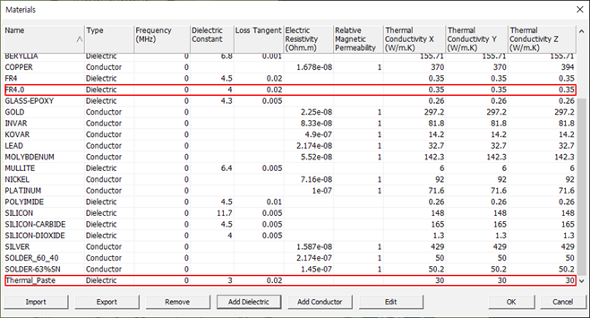
From the menu bar, click Properties > Material Library.
The Materials dialog displays.
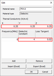
Add FR4.0.
Click Add Dielectric.
The Edit dialog with empty material
property values displays.
Enter FR4.0 in the Material name field.
Enter 0.35 in the X, Y, Z Thermal Conductivity
field.
Enter 4.0 in the Dielectric Constant
field.
Enter 0.02 in the Loss Tangent field.
Figure 1.
Click OK to close the
dialog.
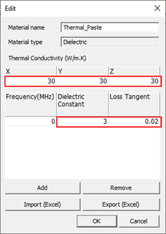
Add Thermal_Paste.
Click Add Dielectric.
The Edit dialog with empty material
property values displays.
Enter Thermal_Paste in the Material name
field.
Enter 30 in the X, Y, Z Thermal Conductivity
field.
Enter 3.0 in the Dielectric Constant
field.
Enter 0.02 in the Loss Tangent field.
Figure 2.
Click OK to close the
dialog.
FR4.0 and Thermal_Paste are registered as new material
names. Figure 3.
Click OK to close the
dialog.
From the menu bar, click File > Save to save the new material library data for the PCB
design.
Build PCB Layer Stack
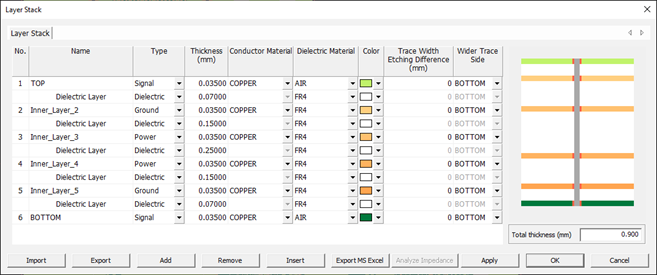
Click Properties > Layer Stack.
The Layer Stack dialog displays.
Click Import.
The Open dialog displays.
Find the directory path in which your own stack-up file resides.
You will use the
C:\ProgramData\altair\PollEx\<version>\Examples\Solver\Thermal\Stackup\Standard_6L_Stackup.udls
file in the current working directory.
Select Standard_6L_Stackup.udls for a 6-layer
stack-up.
Click Open to import this layer stack.
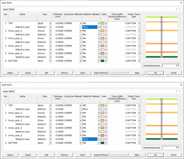
The new stack-up displays, as shown in . Figure 4.
Change dielectric material.
Click and select
FR4.0.
Click and select
FR4.0.
This changes the dielectric materials for Top and Bottom layers to
FR4.0 from FR4, effectively changing the dielectric constant to 4.0 from
4.5. Figure 5.
Click OK to close the
dialog.
From the menu bar, click File > Save to save the new stack-up information.
Define Thermal Properties of DDR3 Memory Device
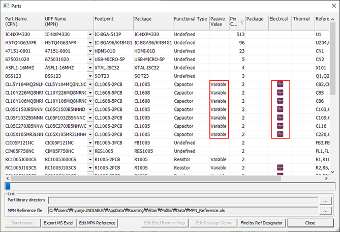
From the menu bar, click Properties > Parts.
The Parts dialog displays.
The passive component
RLC values are automatically extracted from the design database (.pdbb) if
the Value Property has been correctly assigned in the database.
Figure 6.
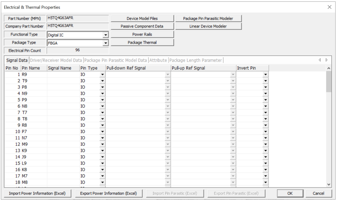
Double-click H5TQ4G63AFR.
The Electrical & Thermal Properties dialog
displays. Figure 7.
Click at Functional Type and select Digital IC.
Click at Package Type and select FBGA.
Click Package Thermal.
The Package Thermal dialog opens.
Enter 1.5 in the Max power dissipation field.
Enter 7.5 in the Body size X field.
Enter 13.3 in the Body size Y field.
Enter 0.73 in the Body height field.
Enter 0.37 in the Mounting height field.
Enter 0.2 in the Pin width field.
Enter 0.37 in the Pin thickness field.
Figure 8.
Click Model Data and check if the default thermal
resistance model data is defined.
Click Cancel to close the Two-Resistor
Model dialog.
Click OK to close the
Package Thermal dialog.
Click OK to close the
Electrical & Thermal Properties dialog.
The Thermal icon displays for H5TQ4G63AFR.
Define Thermal Properties of Controller Device
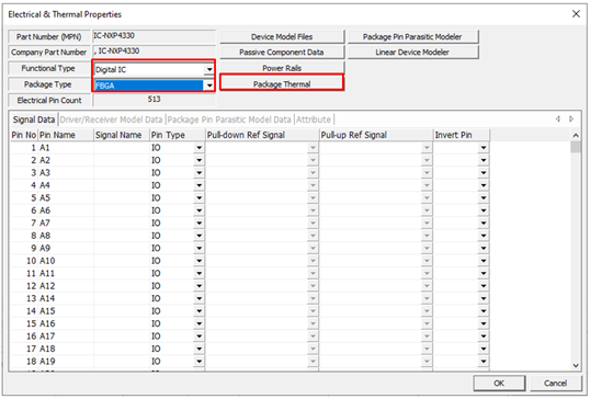
In the Parts dialog, double-click
IC-NXP4330.
The Electrical & Thermal Properties dialog
displays.
Click at Functional Type and select Digital IC.
Click at Package Type and select FBGA.
Figure 9.
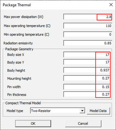
Click Package Thermal.
The Package Thermal dialog displays.
Enter 2.8 in the Max power dissipation field.
You do not have to enter the following geometry data if you want to use the
defaults.
Enter 17 in the Body size X field.
Enter 17 in the Body size Y field.
Enter 0.937 in the Body height field.
Enter 0.27 in the Mounting height field.
Enter 0.15 in the Pin width field.
Enter 0.27 in the Pin thickness field.
Figure 10.
Click Model Data and check if the default thermal
resistance model data are defined.
Click Cancel to close the Two-Resistor
Model dialog.
Click OK to close the
Package Thermal dialog.
Click OK to close the
Electrical & Thermal Properties dialog.
You can now see Thermal in IC-NXP4330.
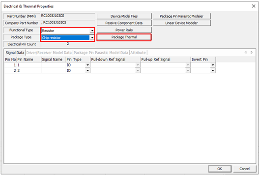
Define Thermal Properties of Passive Component
In the Parts dialog, double-click
RC1005J103CS.
The Electrical & Thermal Properties dialog
displays.
Click at Functional Type and select Resistor.
Click at Package Type and select Chip resistor.
Figure 11.
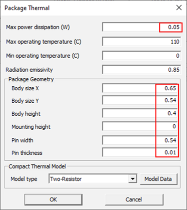
Click Package Thermal.
The Package Thermal dialog displays.
Enter 0.05 in the Max power dissipation field.
You do not have to enter the following geometry data if you want to use the
defaults.
Enter 0.65 in the Body size X field.
Enter 0.54 in the Body size Y field.
Enter 0.4 in the Body height field.
Enter 0 in the Mounting height field.
Enter 0.54 in the Pin width field.
Enter 0.01 in the Pin thickness field.
Figure 12.
Click Model Data and check if the default thermal
resistance model data is defined.
Click Cancel to close the Two-Resistor
Model dialog.
Click OK to close the
Package Thermal dialog.
Click OK to close the
Electrical & Thermal Properties dialog.
You can now see Thermal in RC1005J103CS.
Click Close to close the Parts
dialog.
From the menu bar, click File > Save to save the new part property data.
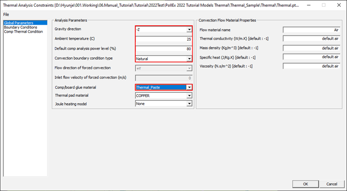
Define Global Thermal Analysis Parameters
From the menu bar, click Analysis > Thermal > Thermal Analysis Constraints.
The Thermal Analysis Constraints dialog
displays.
Select Global Parameters.
Click at Gravity Direction and select -Z.
It is assumed that the PCB is placed on the floor with the component placed
side facing up.
Enter 25 in the Ambient temperature field.
Enter 80 in the Default comp analysis power level
field.
Click at Convection boundary condition type and select
Natural.
It is assumed that natural air circulation is used to cool off the PCB
assembly instead of using a fan.
Click at Comp/board glue material and select
Thermal_Paste.
Figure 13.
Click OK to close the
Thermal Analysis Constraints dialog.
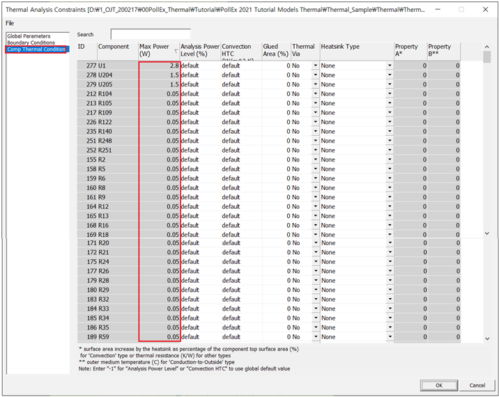
Review Component Thermal Condition
From the menu bar, click Analysis > Thermal Analysis > Thermal Analysis Constraints.
The Thermal Analysis Constraints dialog
displays.
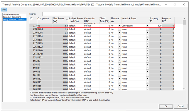
Select Comp Thermal Condition.
Figure 14.
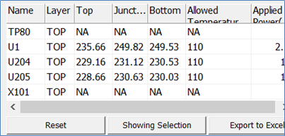
The maximum power defined for component U1 is 2.8W while 1.5 W has been
defined for each of the components U204 ~ U205 and 0.05 W for all resistors R2 ~
R32. For analysis power level, you will use the global default value (80%)
specified in Define Global Thermal Analysis Parameters. No
localized thermal condition will be considered for all components.
Click OK to close the
Thermal Analysis Constraints dialog.
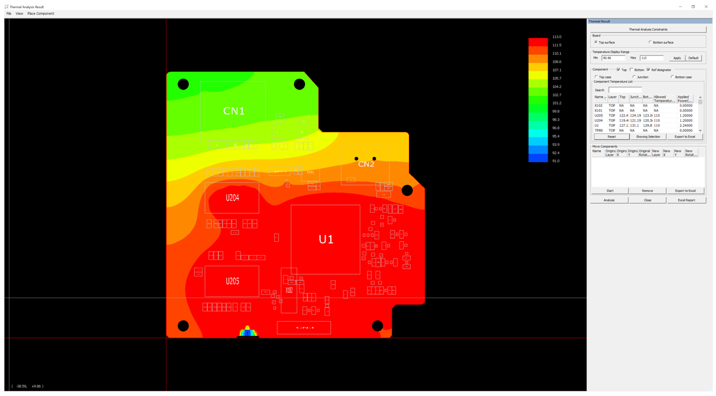
Run Thermal Analysis
From the menu bar, click Analysis > Thermal Analysis > Thermal Analyzer to launch the thermal analyzer.
After running the analysis, the analysis results display.
Enter 113 for Max Temperature Display Range.
Click Apply.
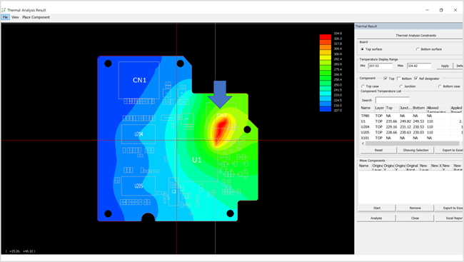
Place mouse cursor on a board location.
Temperatures along X and Y directions display at the bottom and left sides of
the window. At the right side of the window, you can check the listed component
junction temperatures exceeding allowed.Figure 15.
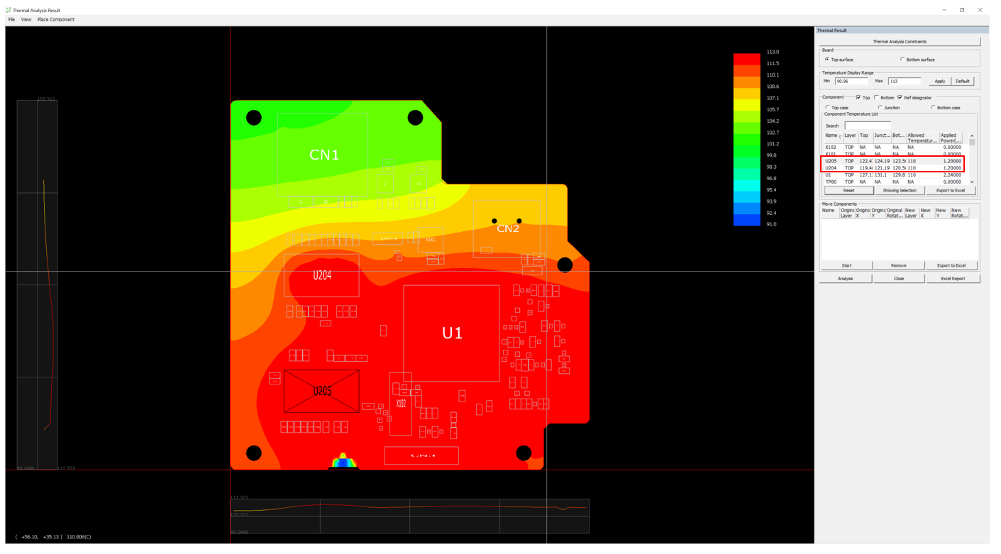
Double-click any component to review its top, bottom, and junction
temperatures.
In the right-side component temperature table, the selected component data is
highlighted. Figure 16.
From the menu bar, click File > Save As to save the analysis result.
Navigate to your current working directory and save it using the default file
name.
From the menu bar, click File > Load to re-load the saved simulation result.
Select the saved file and open it.
From the menu bar, click File > Exit to close the Thermal Analysis Result
dialog.
Correct Thermal Problems
Review the results.
From the menu bar, click Analysis > Thermal > Analysis Result.
The Windows Explorer dialog
opens.
Select the PollEx_PCB_Sample_r1.pthr file and
open it.
The Thermal Analysis Result dialog
displays.
Enter 113 for Max Temperature Display
Range.
Click Apply.
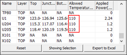
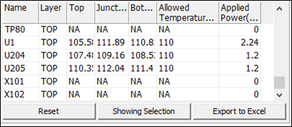
Component junction temperatures exceeding the allowable temperature of
110 degrees can be found. You will resolve the problem by attaching a
component heat-sink. Figure 17.
Attach component heat-sinks.
In the Thermal Analysis Result window, click Thermal
Analysis Constraints to open the Thermal
Analysis Constraints dialog.
Click the Comp Thermal Condition tab.
Click for Heatsink Type of U1 and select
Convection.
The Heatsink Type - Property dialog displays.
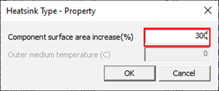
Enter 300 for Component surface area
increase.
By attaching the heat-sink, 300 percent of the original component top
surface area is added to the component top surface. Figure 18.
Click OK to close the
Heatsink Type - Property dialog.
Click OK to close the
Thermal Analysis Constraints dialog.
In the Thermal Analysis Result dialog, click
Analysis to re-run and get new analysis
results.
Upon completion of thermal analysis, new results display, as
shown in the figure.
Enter 113 for Enter Max Temperature Display
Range.
Click Apply.
The junction temperatures of all major ICs meet the requirement. Figure 19.
From the menu bar, click File > Save As to save the analysis result.
Enter Thermal_Sample_with_heatsink.pthr for the
file name.
From the menu bar, click File > Exit to close the Thermal Analysis Result
dialog.
Add Joule Heating
Pre-processing.
From the menu bar click Analysis > Thermal > Joule Heating.
The Joule Heating Analysis dialog
opens.
Click Select Net.
The Select Net dialog opens.
Select the VCC1P0_USB net and click
OK.
In the Joule Heating Analysis dialog, click
Ports.
The Joule Heating Ports dialog
opens.
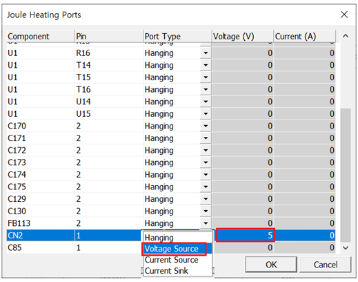
Select CN2, and select Voltage
Source as a Port Type, and enter
5 in the Voltage.
Figure 20.
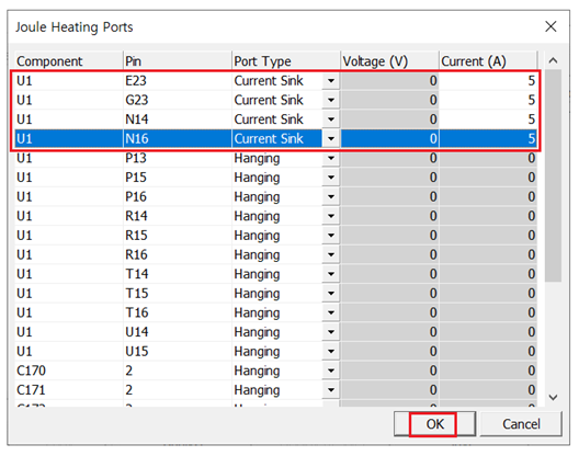
Select the Port Type of U1-E23,
G23, N14, and
N16 as Current Sink and enter
5 in each Current.
Figure 21.
Click OK to close the
Joule Heating Ports dialog.
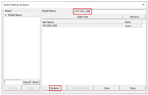
In the Joule Heating Analysis dialog, enter
VCC1P0_USB as a Model Name.
Click Analyze to analyze this structure.
Figure 22.
When analysis is finished, the Joule Heating Analysis
Result Display dialog opens.
Review the result and close the Joule Heating Analysis Result
Display dialog.
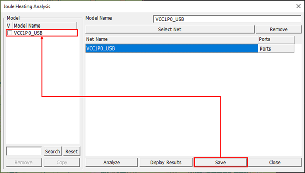
In the Joule Heating Analysis dialog, click
Save to save this result.
Figure 23.
Click Close to close the Joule Heating
Analysis dialog.
Thermal analysis with Joule Heat.
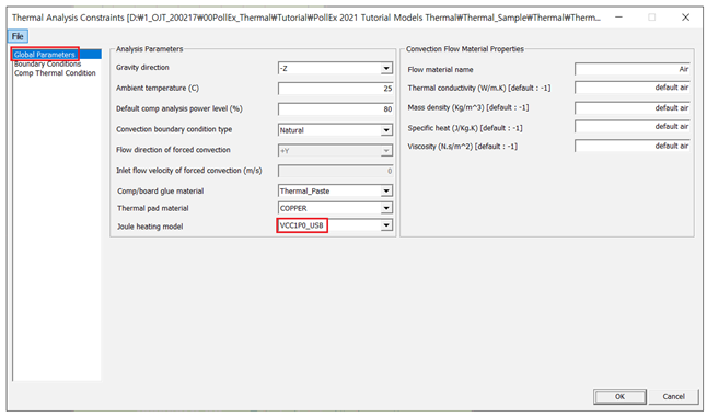
In the PDBB dialog, click Analysis > Thermal > Thermal Analysis Constraints menu.
The Thermal Analysis Constraints dialog
opens.
In the Global Parameters tab, select VCC1P0_USB
as a Joule heating model.
Figure 24.
In the Comp Thermal Condition tab, check whether the setup of
Convection Type Heatsink is maintained in U1 component.
Figure 25.
Click OK to close the
Thermal Analysis Constraints dialog.
In the PDBB dialog, click Analysis > Thermal > Thermal Analyzer menu.
When the analysis is finished, the Thermal analysis
Constraints dialog opens.
Review the Joule Heat results.
Looking at the result map, you can see the Joule Heat temperature of
VCC1P0_USB net.
Figure 26.
Comparing the table on the right, you can see that the temperature of
the surrounding IC increased due to Joule Heat of VCC1P0_USB net.
Figure 27.
Click Close to close the Thermal
Analysis Result dialog.
 and select
FR4.0.
and select
FR4.0.