MCP Tutorial
Assign MCP Model to the Memory
-
Click Pin Count twice to sort the results.
The passive component RLC values are automatically extracted from PDBB data if the value property was correctly assigned in the PDBB database.
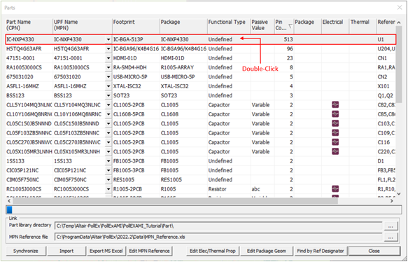
Figure 1. -
Double-click IC-NXP4330.
The Electrical & Thermal Properties dialog displays.
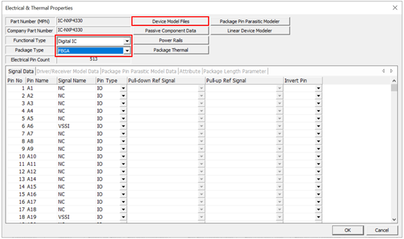
Figure 2. -
Click Device Model Files.
The Device Model Files dialog displays.
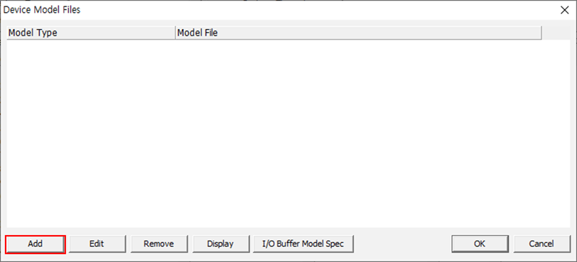
Figure 3. -
For Model type, select EBD.
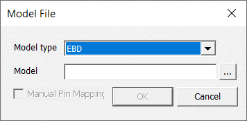
Figure 4. -
Click
 to search and select the EBD file
(C:\ProgramData\altair\PollEx\<version>\Examples\Solver\SI\Simulation_Model\j9k8_j9k9_254b.ebd)
for Memory and click Open to add EBD and the relevant
files (IBIS and Package Parasitic).
to search and select the EBD file
(C:\ProgramData\altair\PollEx\<version>\Examples\Solver\SI\Simulation_Model\j9k8_j9k9_254b.ebd)
for Memory and click Open to add EBD and the relevant
files (IBIS and Package Parasitic).
-
To close the Device Model Files dialog, click
OK.
When the IBIS file contains numbers of different pin count, the message like below is popped up. In this case, you click Yes.
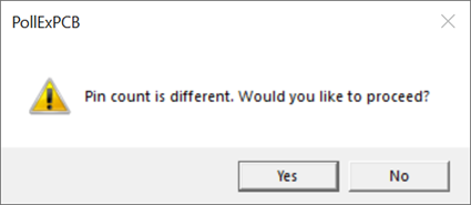
Figure 5.The Device Model Files dialog displays. The EBD, IBIS, and Package Parasitic are displayed.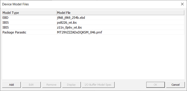
Figure 6. -
Select the Package Parasitic and click Display to view
the Package Pin Parasitic Modeler.
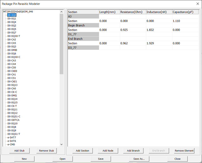
Figure 7. -
Select the IBIS file (z11n_0p6v_wt.ibs) as a memory IBIS
model.
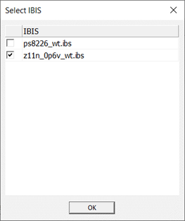
Figure 8. -
Click Package Pin Parasitic Model Data tab. Click
MCP Reset to verify the detailed information for each
pin.
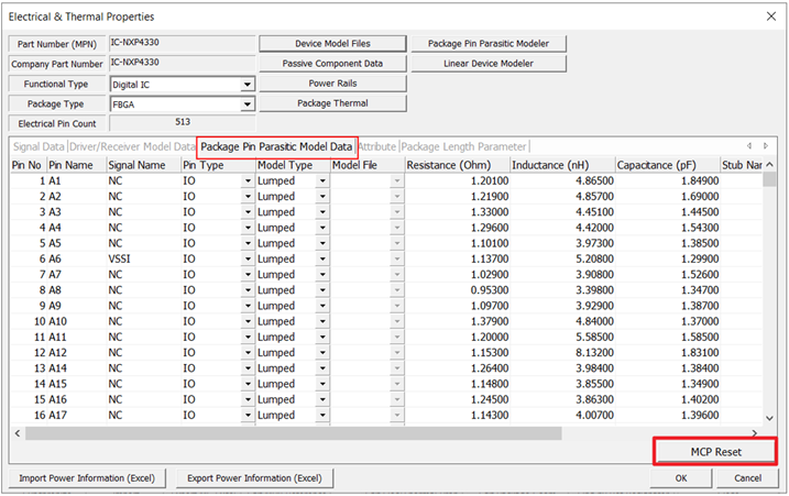
Figure 9. -
Select the Package Pin Parasitic file
(MT29VZZZADxDQKSM_046.pmf) and click
OK.
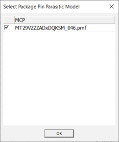
Figure 10.
Assign MCP Model to Controller
-
Click Pin Count twice to sort the results.
The passive component RLC values are automatically extracted from PDBB data if the value property was correctly assigned in the PDBB database.
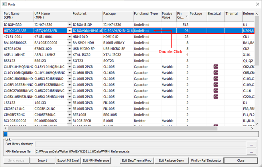
Figure 11. -
Double-click H5TQ4G63AFR.
The Electrical & Thermal Properties dialog displays.
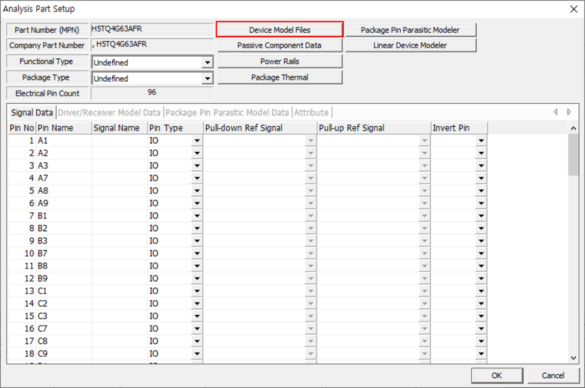
Figure 12. -
Click Device Model Files.
The Device Model Files dialog displays.
Figure 13. -
Click to search and select the IBIS file
(C:\ProgramData\altair\PollEx\<version>\Examples\Solver\SI\Simulation_Model\Memory.ibs)
for Controller device and click Open to open this file
and close this Explorer window.
-
To close the Device Model Files dialog, click
OK.
When the IBIS file contains numbers of different components (IC devices), you need to select one of them. Pin count can be a good reference to select the right one.The Select Component dialog displays.
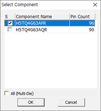
Figure 14. -
Click OK to close the Electrical & Thermal
Properties dialog.
The Electrical icon appears.
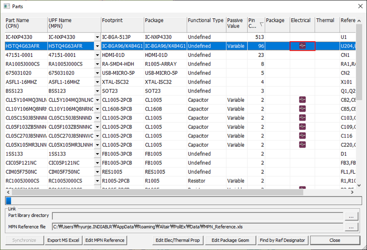
Figure 15.
Explore the Waveform Analysis
-
Click Select Net.
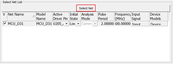
Figure 16. -
Select MCU_D31 and click OK.
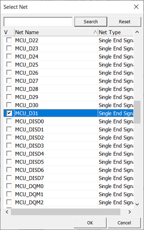
Figure 17. -
Click Device in the Network
Analysis dialog.
Check the connected components and pins to the selected net using the Device Model List dialog.
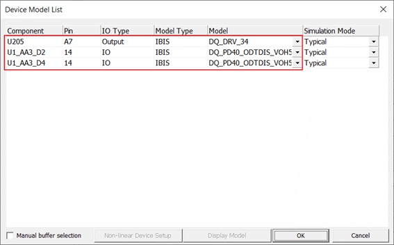
Figure 18. -
Click Analyze.
When the waveform analysis starts, electromagnetic simulation extracts the SPICE model for the selected net. The excitation source signal is applied to the net which is specified by the assigned pin model’s operating characteristics and the values defined at Input Signal and Pulse Period. When the simulation is done, the Waveform Viewer opens or exploring the waveforms.
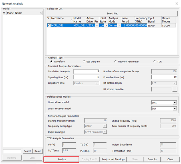
Figure 19.Waveform Viewer dialog opens providing all waveform for TX and RX.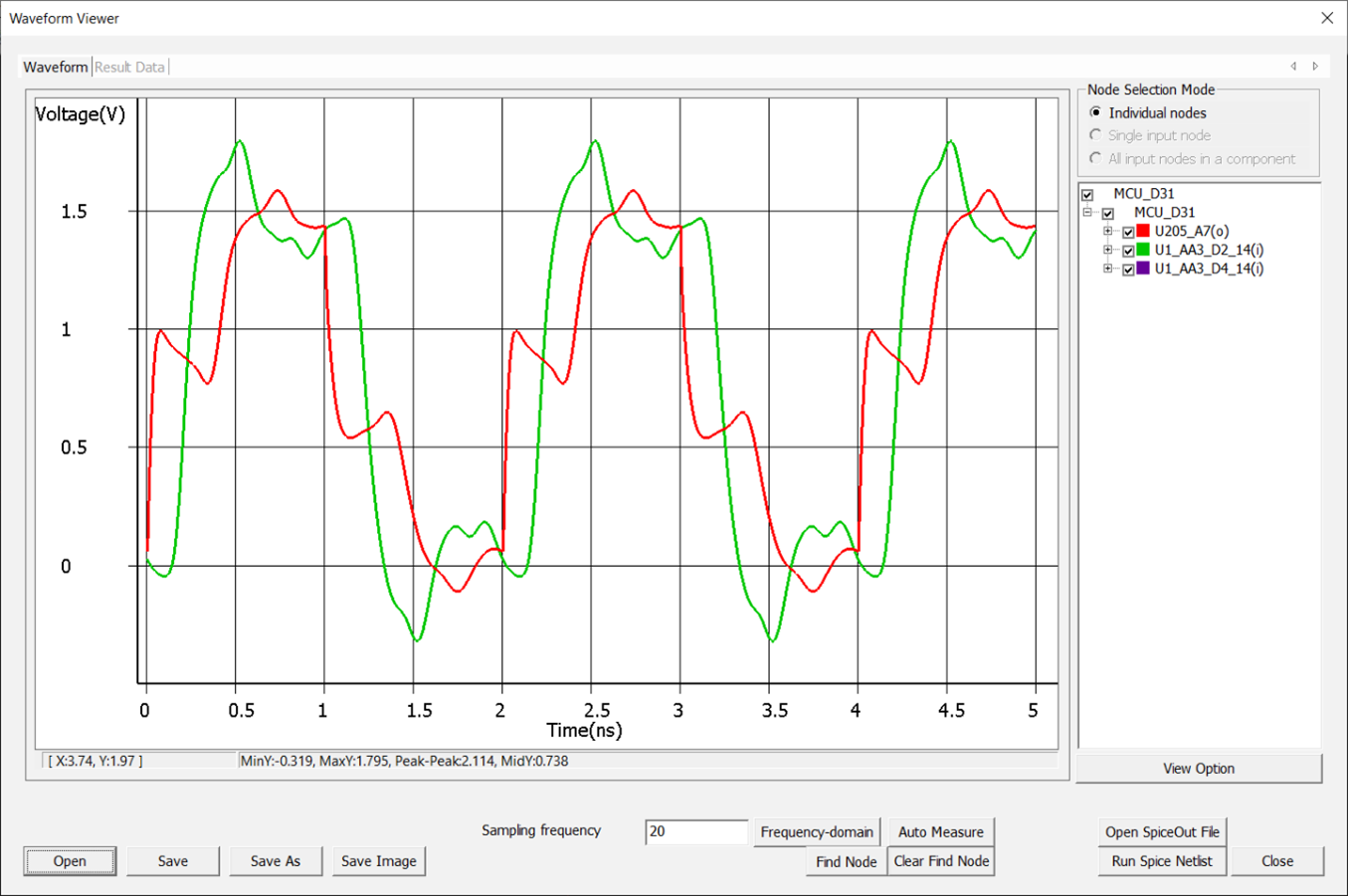
Figure 20.
Explore Eye Diagram Analysis
-
Select the desired net MUC_D31 to analyze.
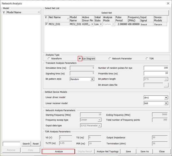
Figure 21. -
Click Analyze.
Waveform Viewer dialog displays.
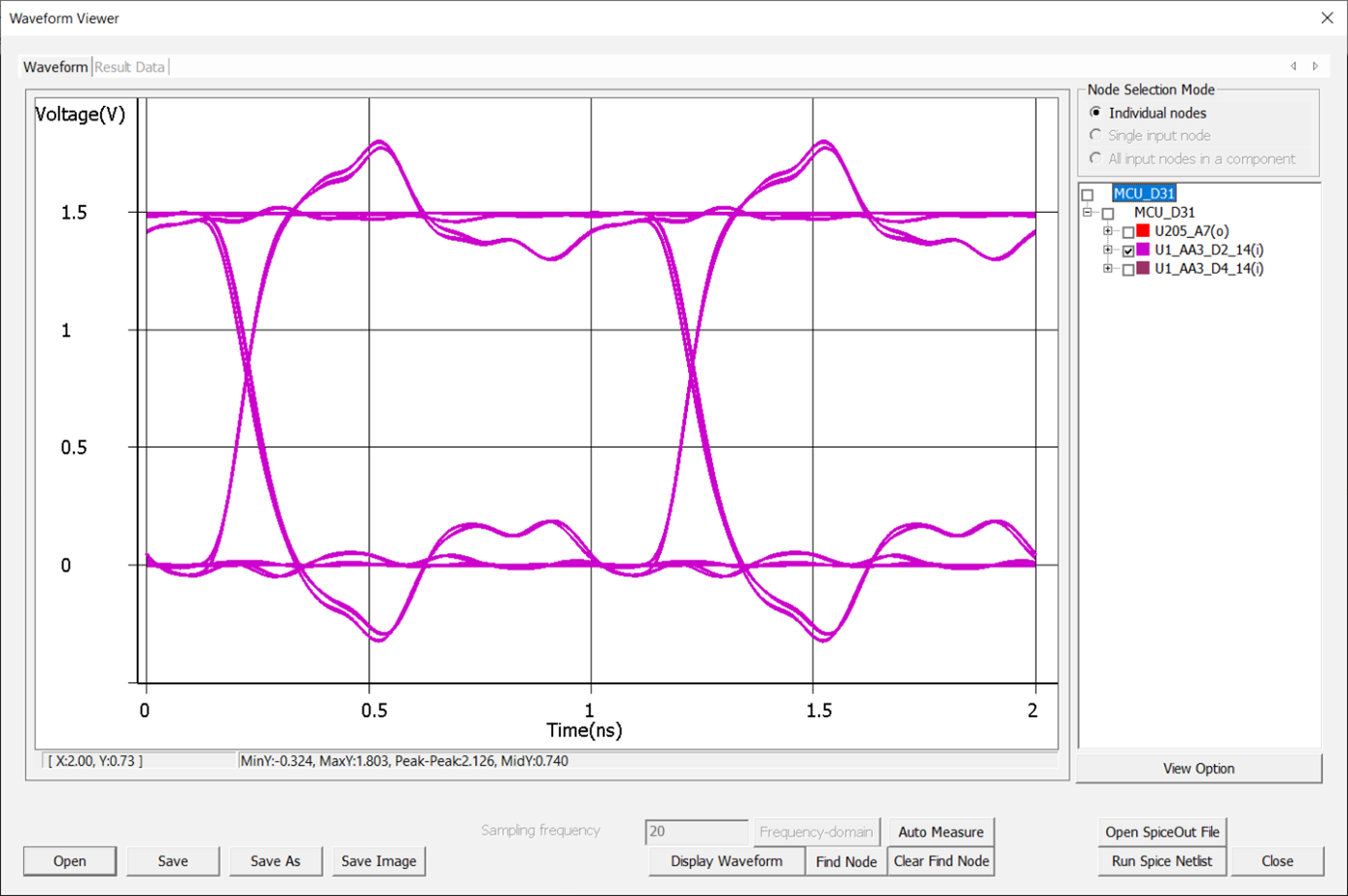
Figure 22.
Analyze Topology
In this step, you will analyze topology from selected netlist.
-
Select the desired net MCU_D31 to analyze.
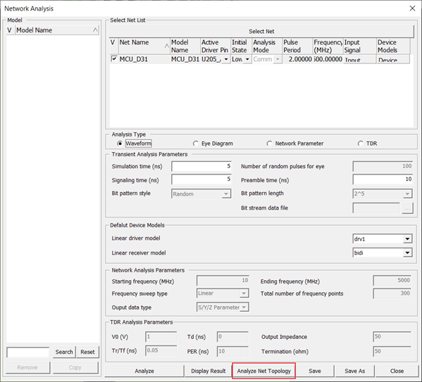
Figure 23. -
Click Analyze Net Topology.
The Net Topology Analyzer dialog opens.
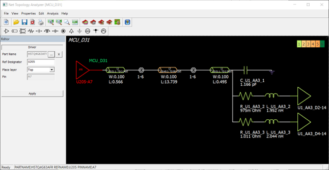
Figure 24. -
Click Select Net.
Figure 25. -
Select MCU_D31 and click OK.
Figure 26. -
Click Device in the Network
Analysis dialog.
Check the connected components and pins to the selected net using the Device Model List dialog.
Figure 27. -
Click Analyze.
When the waveform analysis starts, electromagnetic simulation extracts the SPICE model for the selected net. The excitation source signal is applied to the net which is specified by the assigned pin model’s operating characteristics and the values defined at Input Signal and Pulse Period. When the simulation is done, the Waveform Viewer opens or exploring the waveforms.
Figure 28.Waveform Viewer dialog opens providing all waveform for TX and RX.
Figure 29.