Enter a new design name and select a folder in which the new design folder is
created.
Figure 1.
Click OK.
The SI Explorer dialog opens.
From the menu bar in the SI
Explorer dialog, click Property > Layers.
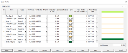
The Layer Stacks dialog opens.
Click Import.
The Explorer dialog opens.
Navigate to the location of the default stack-up files.
The directory location of your own stack-up files:
C:\ProgramData\altair\PollEx\<version>\Examples\Solver\SI\Stackup.
Select the L6_Type1.udls file and click
Open.
Click Open to close the Explorer
dialog.
Our stack-up should now look as shown in . Figure 2.
Click OK to close the
Layer Stacks dialog.
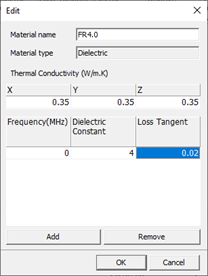
Add New Dielectric Material
In this step, you will add new dielectric material FR4.0.
From the menu bar, click Property > Materials.
The Materials dialog opens.
Click Add Dielectric.
The Edit dialog opens.
For Material name, enter FR4.0.
For the Z, Y, and Z fields, enter 0.35.
For Dielectric Constant, enter 4.0.
For Loss Tangent, enter 0.02.
Figure 3.
Click OK to close to close
Edit dialog.
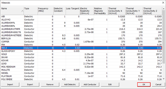
The FR4.0 material is registered as a new material named FR4.0. Figure 4.
Click OK to close to close
Materials dialog.
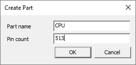
Create Arbitrary Part
In this step, you will create an arbitrary part and assign an IBIS model.
From the menu bar in the SI Explorer dialog, click Properties > Parts.
The Parts dialog opens.
Click Create Part.
The Create Part dialog opens.
For Part name, enter CPU.
For Pin count, enter 513.
Figure 5.
Click OK.
The Electrical & Thermal Properties dialog
opens.
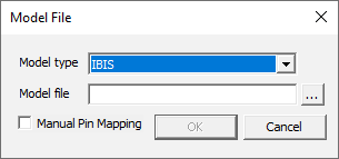
Click Device Model Files.
The Device Model Files dialog opens.
Click Add.
The Model File dialog opens.
For Model type, select IBIS.
Figure 6.
Click .
The Explorer dialog opens.
Navigate to the IBIS model directory and select the
CPU.ibs file from
C:\ProgramData\altair\PollEx\<version>\Examples\Solver\SI\Simulation_Model.
Click Open.
Click OK to close the
Model File dialog.
In the Device Model Files dialog, click
Display.
Figure 7.
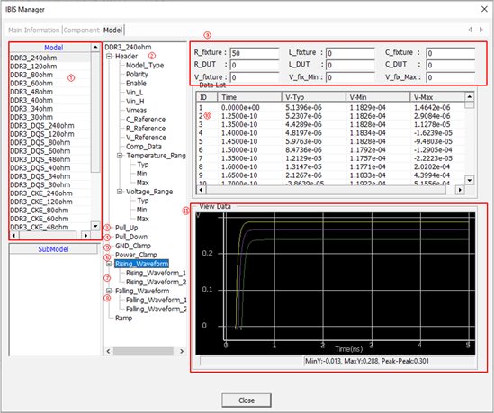
The IBIS Manager dialog opens.
In the Model tab, select DDR3_240ohm.
Review the AC/DC properties.
By exploring the buffer’s AC/DC characteristics, you can choose the proper
buffer model for SI Analysis. Figure 8.
Click Close to close the IBIS Manager panel.
Click OK to close the Device
Model Files panel.
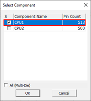
Figure 9.
In the Select Component dialog, select
CPU1 and click OK.
Click OK to close the
Electrical & Thermal Properties dialog.
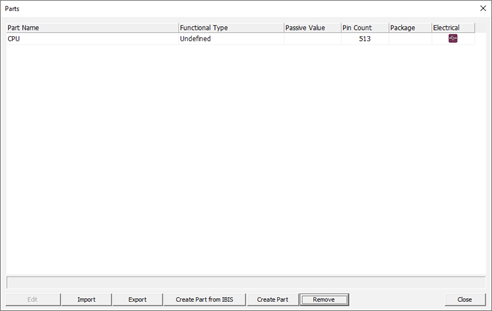
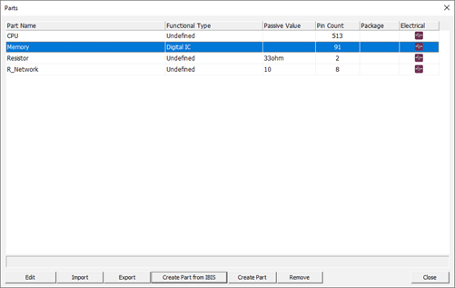
The controller is registered in the Parts
dialog. Figure 10.
Click Close to close the Parts panel.
Create Arbitrary Passive Part
In this step, you will create an arbitrary passive part and assign RLC
model.
From the menu bar, click Properties > Parts.
The Parts dialog opens.
Click Create Part.
The Create Part dialog opens.
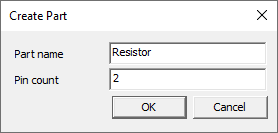
For Part name, enter Resistor.
For Pin count, enter 2.
Figure 11.
Click OK.
The Electrical & Thermal Properties dialog
opens.
Click Passive Component Data.
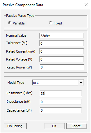
The Passive Component Data dialog opens. Figure 12.
For Nominal Value, enter 33ohm.
For Resistance (Ohm), enter 33.
Click OK to close the
Passive Component Data dialog.
Click OK to close the
Electrical & Thermal Properties dialog.
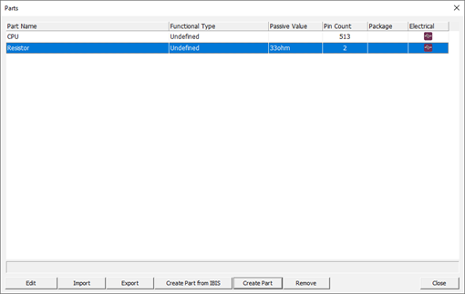
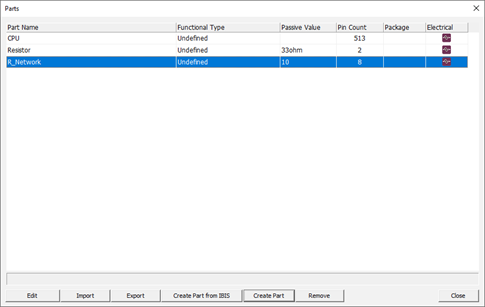
The resistor is registered in the Parts panel. Figure 13.
Click Close.
Assign Passive Component Data
From the menu bar, click Properties > Parts.
The Parts dialog opens.
Click Create Part.
The Create Part dialog opens.
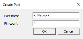
For Par name, enter R_Network.
For Pin count, enter 8.
Figure 14.
Click OK.
The Electrical & Thermal Properties dialog
opens.
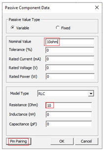
Click Passive Component Data.
The Passive Component Data dialog
opens.
For Nominal Value, enter 10ohm.
For Resistance (Ohm), enter 10.
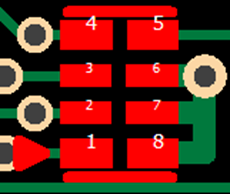
When a passive is an array component, you must define the pin pair
configuration.
Figure 15.
Figure 16.
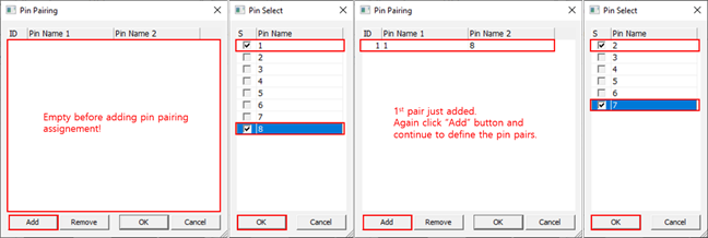
Click Pin Pairing.
The Pin Paring dialog opens.
Click Add.
The Pin Select dialog opens.
Select pin name 1 and 8 as the first pin pair.
Click OK.
Repeat steps 10 -
12 to define
the remaining three pin pairs.
The specified passive component values will be assigned separately to these
paired pins. Figure 17.
Click OK to close the Pin
Paring panel.
Click OK to close the
Passive Component Data dialog.
Click OK to close the
Electrical & Thermal Properties dialog.
The resistor is registered in the Parts dialog. Figure 18.
Click Close to close the Parts
dialog.
Create Part Using IBIS Model
From the menu bar, click Properties > Parts.
The Parts dialog opens.
Click Create Part from IBIS.
The Explorer dialog opens.
Open the Memory.ibs file.
The Electrical & Thermal Properties dialog
opens.
Click OK to close the
Electrical & Thermal Properties dialog.
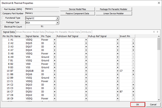
Figure 19.
The new part is created. Figure 20.
Click Close to close the Parts panel.
Import Parts from Previous Design PDBB
From the menu bar, click Properties > Parts.
The Parts dialog opens.
Click Import.
The Explorer dialog opens.
Navigate to the UPF directory:
C:\ProgramData\altair\PollEx\<version>\Examples\UPFs.
Click OK to import the UPF
directory contents.
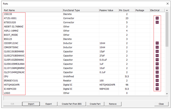
The Parts dialog opens. Every part in the
upfs/Parts directory is imported. Figure 21.
Click Close in the Parts
dialog.
From the menu bar, click File > Save to save this design.
From the menu bar, click File > Close to close this design.
Import PDBB Design File
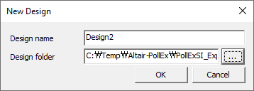
In the SI Explorer dialog, click File > New.
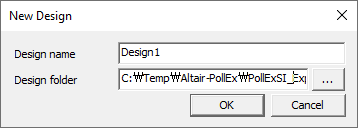
The New Design dialog opens.
Enter a new design name and select a folder in which the new design folder will
be created.
Figure 22.
Click OK to create new design
project.
In the SI Explorer dialog, click File > Import from thePollEx PCB.
The Explorer dialog opens.
Select the PollEx_New_Sample.pdbb file and click
Open.
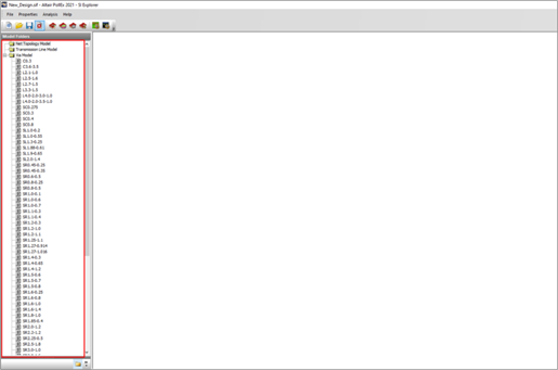
The imported transmission line models, Via Models, and net topology
models are listed in the SI Explorer dialog. Figure 23.
After importing, you must assign a simulation model. Here, you will use
the import method from the unified part library.
In the SI Explorer dialog, click Properties > Part.
The Part dialog opens.
Click Import.
The Explorer dialog opens.
Navigate to the UPF directory and click OK to import UPF directory contents.
Close the Part dialog.
Extract Transmission Line Properties
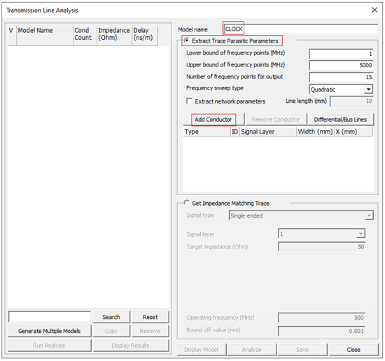
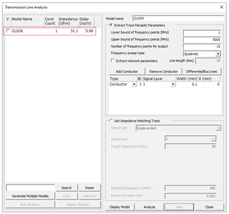
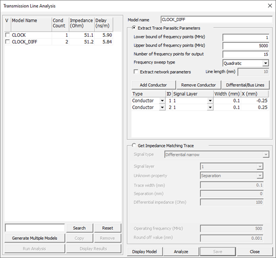
In the SI Explorer dialog, click Analysis > Transmission Line Analysis.
The Transmission Line Analysis dialog
opens.
For Model name, enter CLOCK.
Figure 24.
Select Extract Trace Parasitic Parameters.
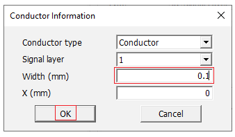
Click Add Conductor.
The Conductor Information dialog
opens.
For Width, enter 0.1.
Figure 25.
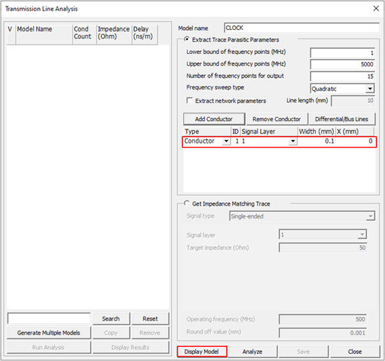
Click OK.
The created transmission line model is displayed in the model
field.
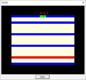
Click Display Model at the bottom of the
Transmission Line Analysis dialog.
Figure 26.
The CLOCK dialog opens.
Verify the stack up and trace shape and click
Close.
Figure 27.
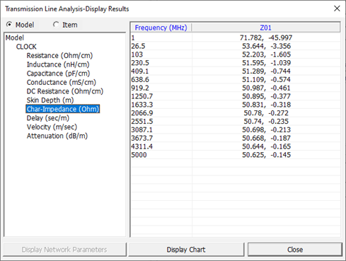
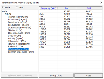
Click Analyze.
The Transmission Line Analysis-Display Results
dialog opens. The default properties shown on the right side are Char-Impedance.
You can switch the property display by clicking other characteristic. Figure 28.
Click Close.
Click Save.
The CLOCK model is registered in the Model Name window. Figure 29.
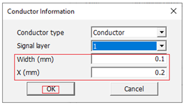
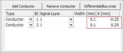
Click Add Conductor.
The Conductor Information dialog
opens.
For Width (mm), enter 0.1.
For X (mm), enter 0.2.
Click OK.
X represents the distance between the centers of two traces. Figure 30.
In the Transmission Line Analysis-Display Results dialog,
click Display Model.
Verify the stack up and trace shape and click
Close.
Two traces will be located at the same signal layer numbered as 1.
Click Analyze.
The Transmission Line Analysis-Display Results
dialog opens. The analyzed properties shown at right side are
Diff-Impedance.
Click characteristics to switch the property display.
Click Close.
Figure 31.
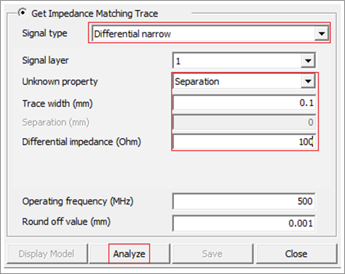
Get Impedance Matching Trace
In the Transmission Line Analysis dialog, enter
CLOCK_Diff for the Model name.
Select Get Impedance Matching Trace.
For Signal type, select Differential narrow.
For Unknown property, select Separation.
For Trace width (mm), enter 0.1.
For Differential impedance (ohm), enter 100.
Click Analyze.
Figure 32.
In the Transmission Line Analysis-Display Results dialog,
check the calculated Diff-Impedance value.
Click Close.
Figure 33.
Click Save.
Figure 34.
Click Close to close the Transmission Line
Analysis dialog.
Analyze Single-Ended Topology
In the SI Explorer dialog, click Analysis > Net Topology Analysis.
The Net Topology Analyzer dialog
opens.
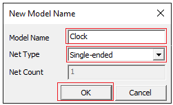
From the Net Topology Analyzer dialog, click File > New.
The Net Model Name dialog opens. Figure 35.
Model Name, enter Clock.
For Net Type, select Single-ended.
Click OK.
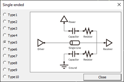
The Single-ended dialog opens.
Select Typ5 which has parallel ac termination and click
Close.
Figure 36.
The Net Topology Analyzer dialog
opens.
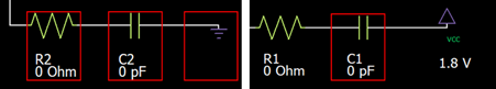
Select R2, C2,
C1, and GND.
Press Delete.
All four elements below are removed. Figure 37.
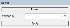
Click VCC.
For Voltage (V), enter 0.75, and click
Apply.
Figure 38.
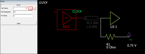
Click U1-1 and click .
Figure 39.
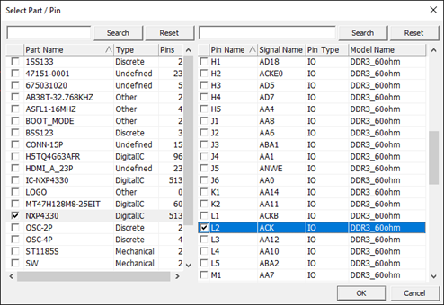
The Select Part/Pin dialog opens.
Enable the NXP4330 and L2
checkboxes.
Figure 40.
Click OK.
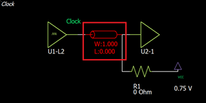
In the Net Topology Analyzer dialog, click the single line
model.
Figure 41.
For Model Name, select CLOCK.
For Length (mm), enter 10.
Click Apply.
Figure 42.
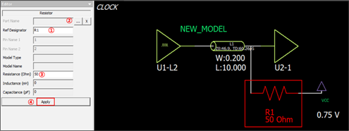
Click R1.
For Resistance, enter 50.
Click Apply.
Figure 43.
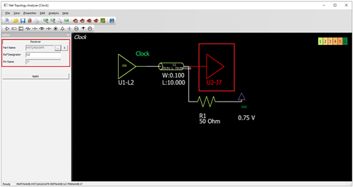
Click U2-1 and click .
The Select Part/Pin dialog opens.
Enable the H5TQ4G63AFR and J7
checkboxes.
Click OK.
Figure 44.
Click Analysis > Network Analysis.
The Topology Network Analysis dialog
opens.
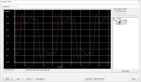
Click Analyze.
The Waveform Viewer dialog opens and displays the
simulated waveform. Figure 45.
Click Close.
From the menu bar, click File > Save As to save this topology.
Save this topology as Clock.ntfb.
Close the Net Topology Analyzer dialog.
Explore Waveform Analysis
In the SI Explorer dialog, click Analysis > Net Topology Analysis.
The Net Topology Analyzer dialog
opens.
Click .
The Net Model Name dialog opens. Figure 46.
For Model Name, enter DDR_Data.
For Net Type, select Single-ended.
Click OK.
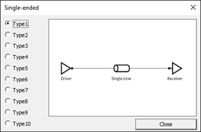
The Single-ended dialog opens.
Select Type1 and click
Close.
Figure 47.
The Net Topology Analyzer dialog
opens.
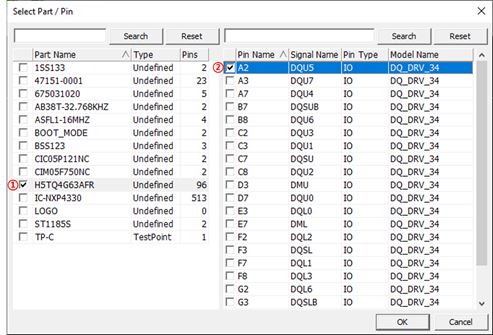
Click U1-1 and click .
Figure 48.
Enable the H5TQ4G63AFR and A2
checkboxes.
Figure 49.
Click OK.
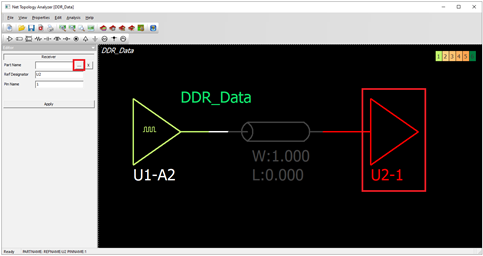
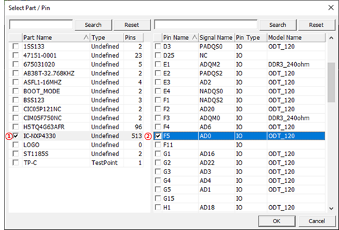
Click U2-1 and click .
Figure 50.
Enable the IC-NXP4330 and F5
checkboxes.
By assigning this pin model, the Receiver will be terminated with 120ohm
resistor described in IBIS file. Figure 51.
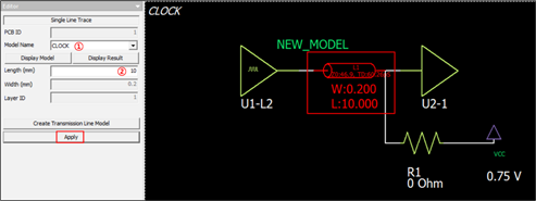
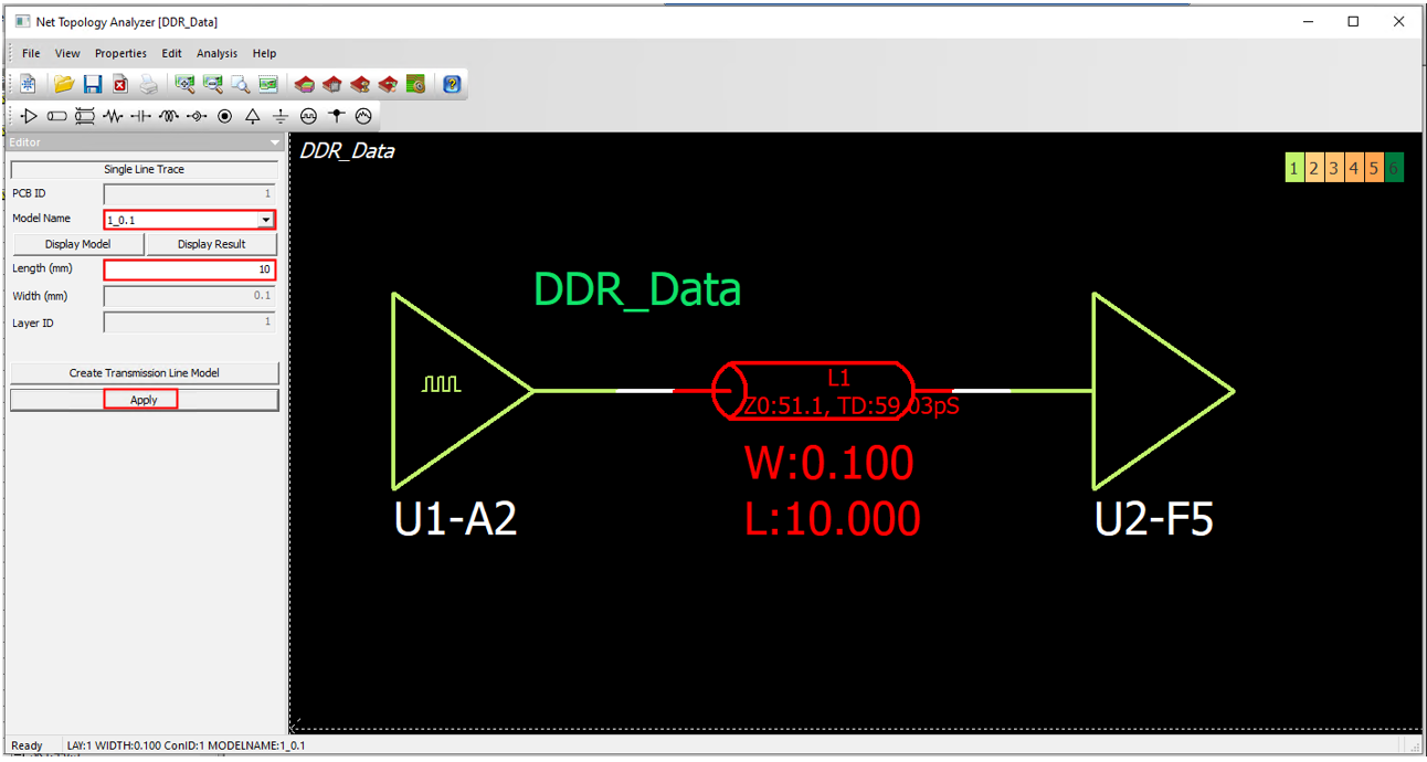
Click single line model and select
CLOCK as the Model Name.
The selected trace model denotes that it is routed at 1 layer with 0.1 (mm)
width. The thickness of the trace and distance to the ground will follow the
stack up information.
Enter 10 as the length.
Click Apply.
Figure 52.
From the menu bar, click File > Save As.
Save this topology as DDR_Data.ntfb.
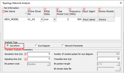
From the menu bar, click Analysis > Network Analysis.
The Topology Network Analysis dialog opens. Figure 53.
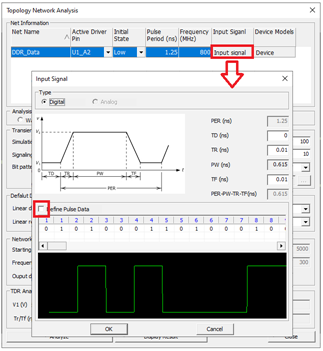
In the Active Driver Pin field, click and select U1_A2.
Device pin model => U1_A2. U2_F5 is the reference pin name of a receiving
device.
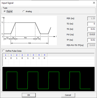
Change the Pulse Period to 1.25 and click
Input Signal.
TD will not change any among Initial State ~ Input Signal, means it just add
specified time as latency of the excitation. 1.25ns pulse will be applied
just after the TD(ns) pauses.
Figure 54.
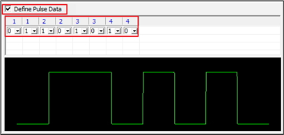
Enable Define Pulse Data checkbox to specify the
switching format.
Figure 55.
Click OK to close the
Input Signal dialog.
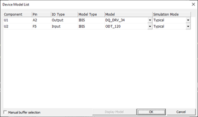
In the Topology Network Analysis dialog, click
Device Models in the Device Models field.
For U1, select DQ_DRV_34 for model.
For U2, select ODT_120 for model and click
OK.
Figure 56.
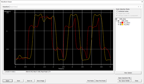
The waveform analysis is ready.
Click Analyze at the bottom of the Topology
Network Analysis dialog.
When the waveform analysis is started, electromagnetic simulation will extract
the SPICE model for the selected net. The excitation source signal will be
applied to the net which is specified by the assigned pin model’s operating
characteristics and the values defined at Input Signal and Pulse Period. When
the simulation is done, the Waveform Viewer dialog will be
displayed as above for exploring the waveforms. Figure 57.
Click Close.
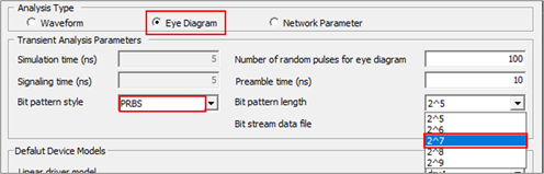
Explore Eye Diagram Analysis
In the Topology Network Analysis dialog, select
Eye Diagram for Analysis Type.
Click Input Signal.
The Input Signal dialog opens.
Disable the Define Pulse Data checkbox and click
OK.
Figure 58.
Select PRBS for Bit Pattern style.
Select 2^7 for Bit pattern length.
All 2^7 numbers of random bit will be applied to the net; the detailed bit
signal pattern will follow the shape defined at Input Signal. Figure 59.
Click Analyze.
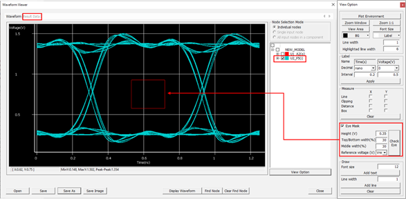
The waveform analysis starts. When the simulation is done, the
Waveform Viewer dialog opens.
In the Waveform Viewer dialog, enable the
U2_F5 checkbox.
Click View Option.
The View Option dialog opens.
Change the value of the Eye Mask region as shown below and click
Check Eye.
Eye mask will come up then move the cursor and click near the center of the eye
pattern.
Figure 60.
Click Close.
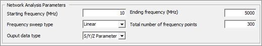
Explore Network Parameter Analysis
In the Topology Network Analysis dialog, select
Network Parameter for Analysis Type.
This enables the S, Y, Z-Parameter extraction to the selected net(s). 300
frequency points will be taken for the parameter extraction. Figure 61.
Click Analyze.
The Network Parameter Viewer dialog
opens.
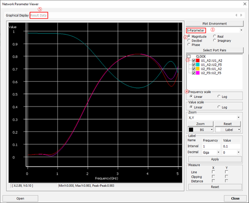
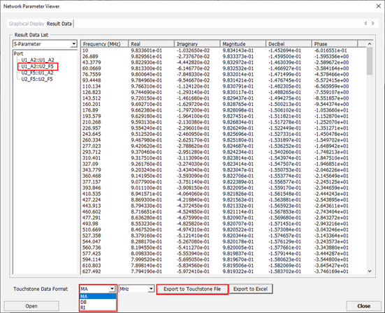
Click Result Data to verify the extracted parameters in
table data format.
Figure 62.
Select Port U1_A2::U2_F5.
Select MA as a Touchstone Data Format.
Click Export to Touchstone File to extract S-Parameters
in Touchstone file format.
 .
The Explorer dialog opens.
.
The Explorer dialog opens.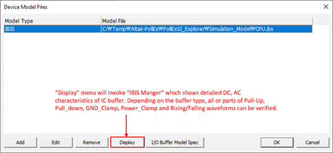
 .
The Net Model Name dialog opens.
.
The Net Model Name dialog opens.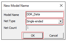
 and select U1_A2.
Device pin model => U1_A2. U2_F5 is the reference pin name of a receiving device.
and select U1_A2.
Device pin model => U1_A2. U2_F5 is the reference pin name of a receiving device.