IBIS-AMI Tutorial
Create Project
Add New Dielectric Material
In this step, you will add a new dielectric material FR4.0 and PSR3.0
-
Click Add Dielectric.
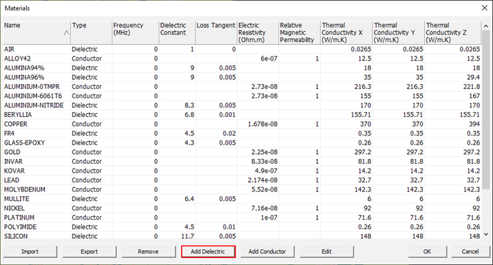
Figure 1.The Edit dialog opens. -
Enter the following values and click OK.
- For the Material name, enter FR4.0.
- For X, Y, and Z, enter 0.35.
- For Dielectric Constant, enter 4.0.
- For Loss Tangent, enter 0.02.
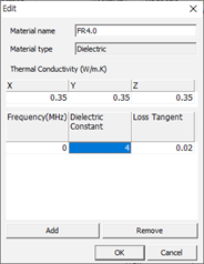
Figure 2. -
Enter the following values and click OK.
- For Material name, enter PSR3.0.
- For X, Y, and Z, enter 0.35.
- For Dielectric Constant, enter 3.0.
- For Loss Tangent, enter 0.02.
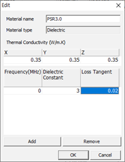
Figure 3.The FR4.0 and PSR3.0 materials are registered as new materials with the names FR4.0 and PSR3.0.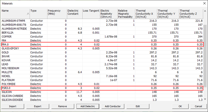
Figure 4. -
Click
 to save this change.
Build PCB Stack
-
In the Layer Stack dialog, click
Import.
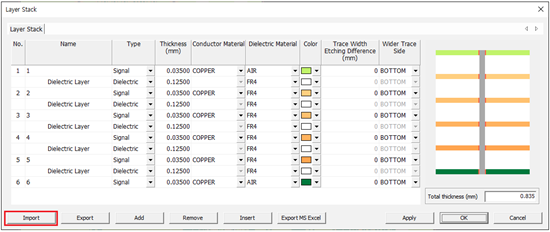
Figure 5. -
Navigate to
C:\ProgramData\altair\<version>\Examples\Solver\SI\Stackup,
select StandardStackup.udls, and click
Open.
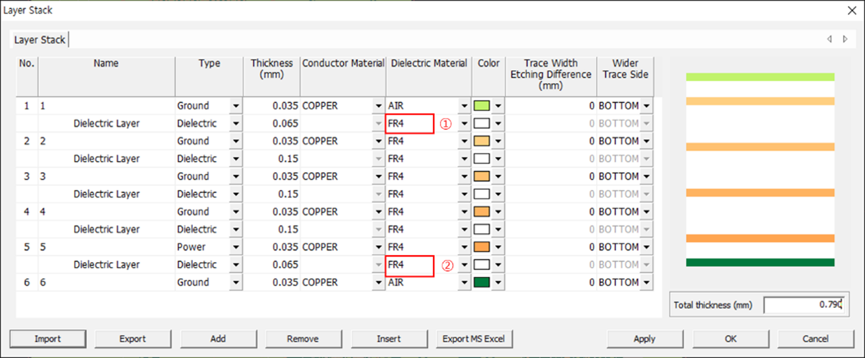
Figure 6. -
Change Dielectric Constant.
-
For the top layer, click
 at 1 and select
FR4.0.
at 1 and select
FR4.0.
-
For the bottom layer, click at 2 and select
FR4.0.
The dielectric constant for the Top and Bottom layers is changed from 4.5 to 4.0.
-
For the top layer, click
-
Add Solder resist layer to the Top and Bottom Layers.
-
For Thickness, enter 0.02.
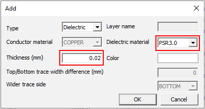
Figure 7. -
Click OK.
The new Solder Resist layer is inserted at the top.
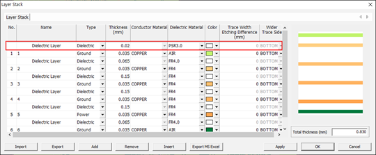
Figure 8. -
For Thickness, enter 0.02.

Figure 9. -
Click OK.
The new Solder Resist layer is inserted at the bottom.
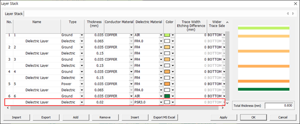
Figure 10.
-
For Thickness, enter 0.02.
-
Click to save this change.
Assign IBIS-AMI Model to Controller
-
Click Pin Count twice to sort the results.
The passive component RLC values are automatically extracted from PDBB data if the value property was correctly assigned in the PDBB database.
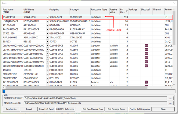
Figure 11. -
Double-click IC-NXP4330.
The Electrical & Thermal Properties dialog displays.
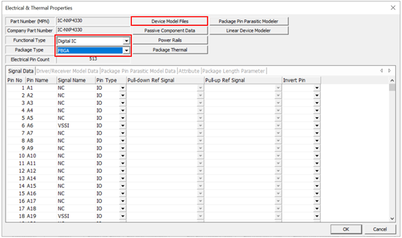
Figure 12. -
Click Device Model Files.
The Device Model Files dialog displays.
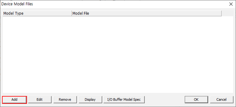
Figure 13. -
Click
 to search and select the IBIS file
(C:\ProgramData\altair\PollEx\<version>\Examples\Solver\SI\Simulation_Model\\test_ibis.ibs)
for Controller and click Open to open this file and close
this Explorer window.
to search and select the IBIS file
(C:\ProgramData\altair\PollEx\<version>\Examples\Solver\SI\Simulation_Model\\test_ibis.ibs)
for Controller and click Open to open this file and close
this Explorer window.
-
To close the Device Model Files dialog, click
OK.
When the IBIS file contains numbers of different pin count, the message like below is popped up. In this case, you click Yes.

Figure 14.The Device Model Files dialog displays. -
Select the first line and click Display to invoke the
IBIS Manager dialog.
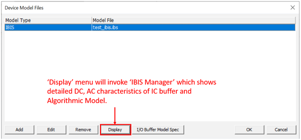
Figure 15.Check the information of IBIS-AMI file in the Main Information tab.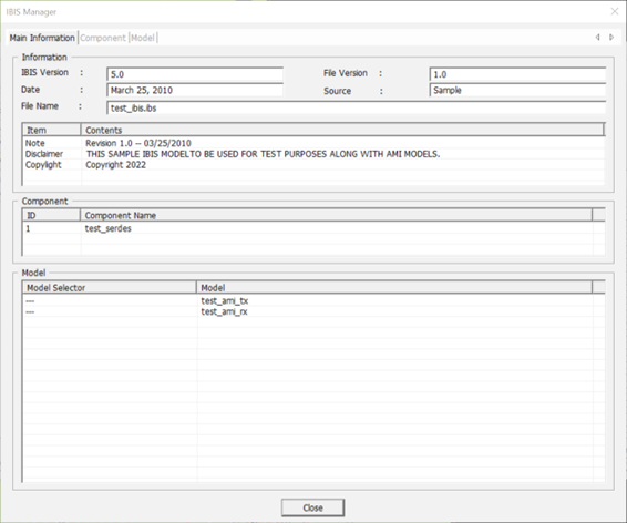
Figure 16. -
Click the Model tab and select Algorithmic
Model.
By exploring the Algorithmic Model, you can check the reserved parameters of IBIS-AMI.
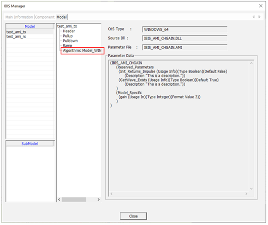
Figure 17.The .ami file must contain a distinct section or sub-tree named 'Reserved_Parameters' beginning and ending with parentheses. The file may also contain another section or sub-tree named 'Model_Specific', beginning and ending with parentheses. The sub-trees 'Reserved_Parameters' and 'Model_Specific' are branches of the root of the tree.
The Model Parameter File must be organized in the following way: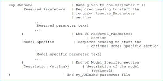
Figure 18. -
Click Driver/Receiver Model Data tab to verify the
detailed information related to I/O buffer assignment for each pin included in
the IC part.
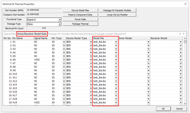
Figure 19. -
Click Package Pin Parasitic Model Data to verify the
Resistance, Inductance, and Capacitance.
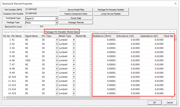
Figure 20. -
Click OK to close the Electrical & Thermal
Properties dialog.
The Electrical icon appears.
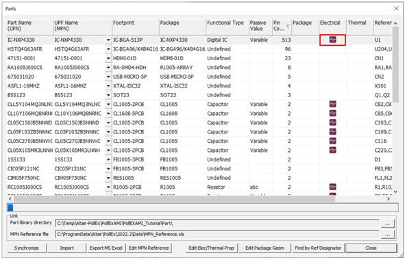
Figure 21. -
Verify the test_ibis.ibs file with two AMI files and two
DLL file in the location <Your sample's working
derectory\Part\IC-NXP4330.
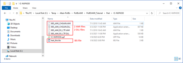
Figure 22.Each AMI model is a combination of an analog model and an algorithmic model and consists of three files: .ibs, .ami and DLL. Analog model is specified in the .ibs file. DLL is the executable of the algorithmic model, whose parameters are specified in the .ami file.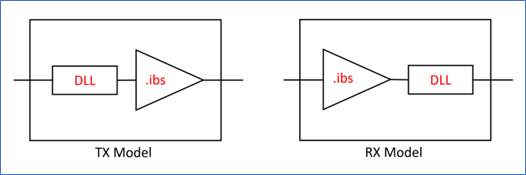
Figure 23.
Assign IBIS-AMI to Connector
-
In the Parts dialog, double-click
675031020.
The Electrical & Thermal Properties dialog displays.
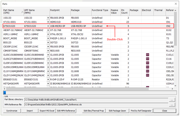
Figure 24. -
Click Device Model Files.
The Device Model Files dialog displays.
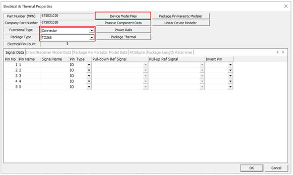
Figure 25. -
Click Add.
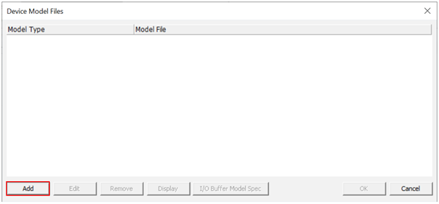
Figure 26. -
Click to search and select the IBIS file
(C:\ProgramData\altair\PollEx\<version>\Examples\Solver\SI\Simulation_Model\test_ibis.ibs)
for Controller device and click Open to open this file
and close this Explorer window.
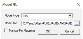
Figure 27. -
Click OK to close the Model Files
dialog.
The Device Model Files dialog displays.
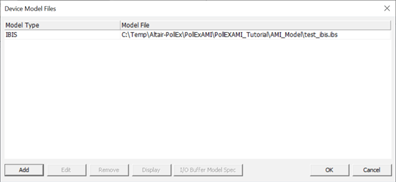
Figure 28. -
To close the Device Model Files dialog, click
OK.
When the IBIS file contains numbers of different pin count, the message like below is popped up. In this case, you click Yes.
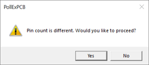
Figure 29.The Electrical & Thermal Properties dialog opens. The connector’s part properties are assigned automatically, as shown in the Electrical & Thermal Properties dialog.The Signal Data, Driver/Receiver Model Data, Package Pin Parasitic Model Data, and Attribute tabs provide detailed information.
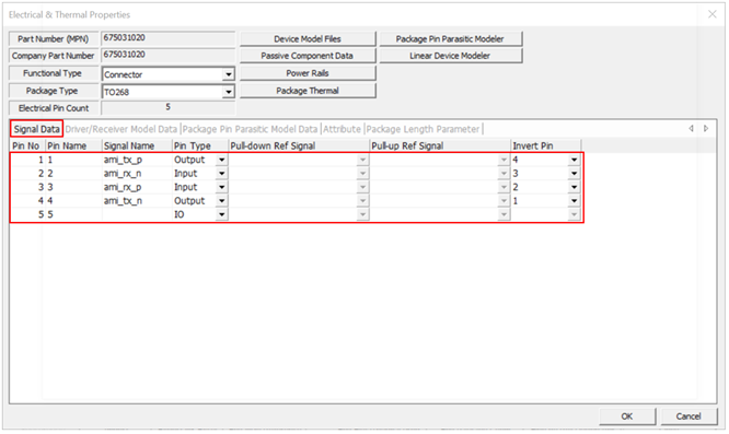
Figure 30. -
Click Driver/Receiver Model Data tab to verify the
detailed information related to I/O buffer assignment for each pin included in
the IC part.
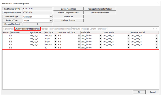
Figure 31. -
Click Package Pin Parasitic Model Data to verify the
Resistance, Inductance, and Capacitance.
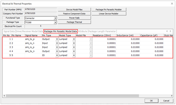
Figure 32. -
Click OK to close the Electrical & Thermal
Properties dialog.
The Electrical icon appears.
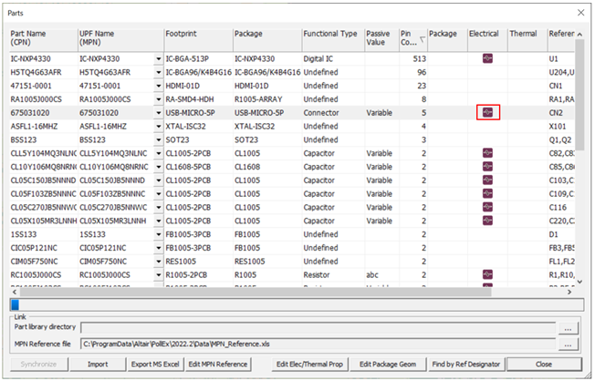
Figure 33. -
Verify the test_ibis.ibs file with two AMI files and two
DLL file in the location <Your Sample's working
derectory\Part\675031020.
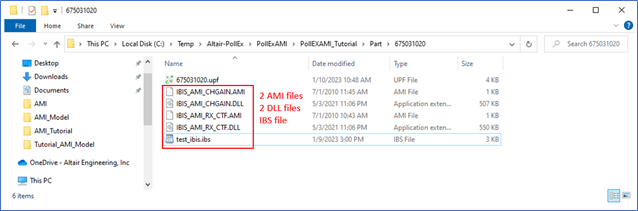
Figure 34.
Assign Passive Component Data to R and C
-
Double-click RC1005J000CS in the
Parts dialog.
The Electrical & Thermal Properties dialog displays.
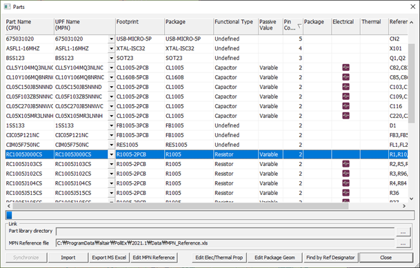
Figure 35. -
Click Passive Component Data in the Electrical
& Thermal Properties dialog.
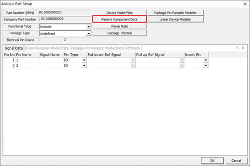
Figure 36. -
For Passive Value Type, select Fixed.
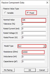
Figure 37.
Assign Net Properties for Power
-
Double-click 5VCC.
The Edit dialog displays.
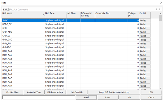
Figure 38. -
For Voltage, enter 5.0.
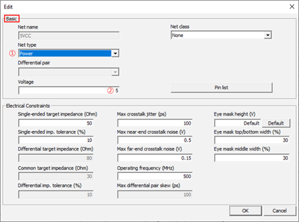
Figure 39.
Assign Net Properties for Differential Pair
-
Double-click MCU_HOST_USB+ net.
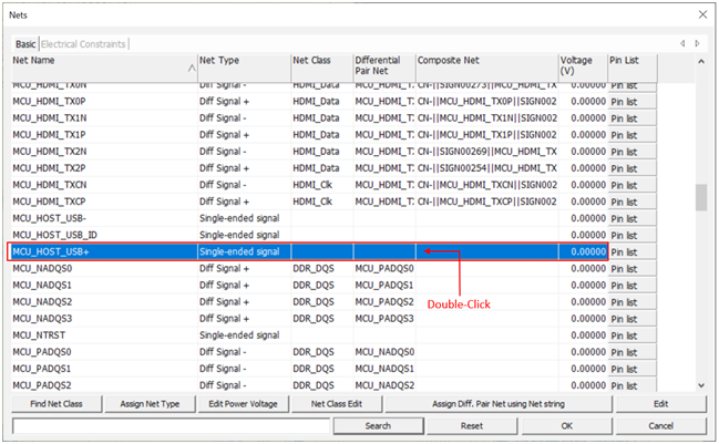
Figure 40.The Edit dialog displays. -
For Net class, select USB2.
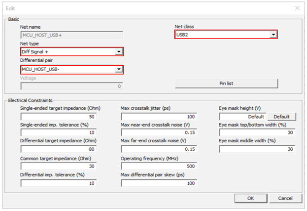
Figure 41. -
Click OK to close the
Edit dialog.
The MCU_HOST_USB+ and MCU_HOST_USB- nets are combined as a differential pair net.
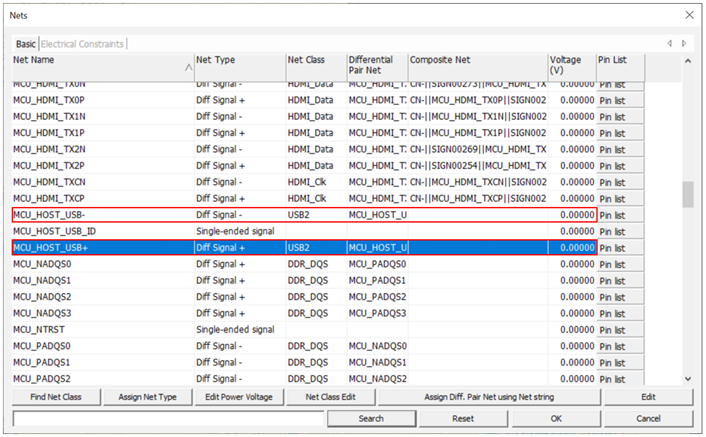
Figure 42.
Assign Net Properties Automatically
-
Click Assign Net Type.
PollEx automatically assigns the Net Type of all nets using the information in the IBIS model and net name string.
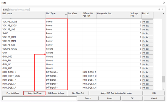
Figure 43. -
Click Find Net Class.
PollEx automatically assigns the Net Class to all nets using pre-defined Net Class Definition. When creating a Net class, if there is a net with duplicate definitions, the following dialog opens.
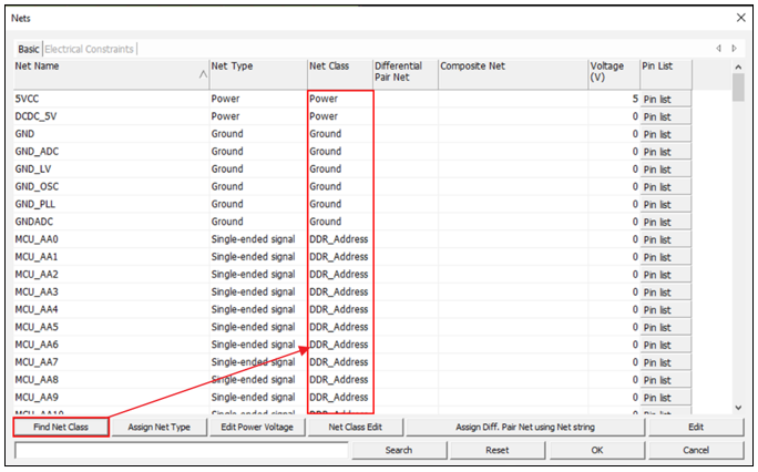
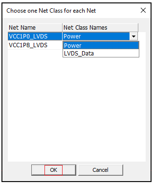
Figure 44.
Create Composite Net
-
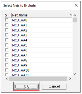
Click Generate Composite Net.
The Selects Nets to Exclude dialog opens. You can specify nets that should not be composited with other nets, such as Power and Ground nets.
-
Click OK and check the listed
composited nets.
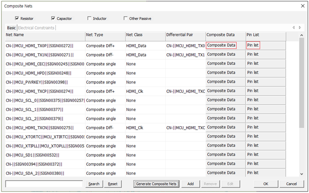
Figure 45. -
Click Composite Data or Pin List
to review composite net structure or the pin list.
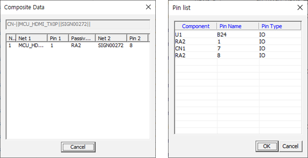
Figure 46. -
Click to save this change.
Explore the Waveform Analysis
-
Click Select Net.
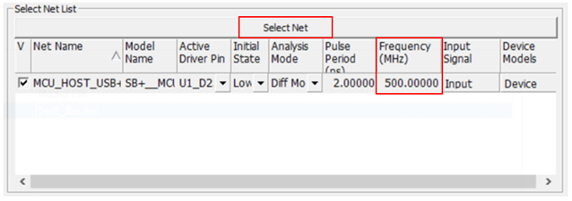
Figure 47. -
Select MCU_HOST_USB+ and click OK.
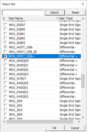
Figure 48. -
Click Device in the Network
Analysis dialog.
Check the connected components and pins to the selected net using the Device Model List dialog.
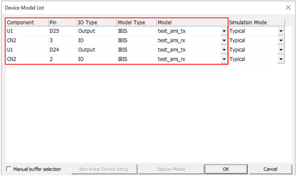
Figure 49. -
Click Analyze.
When the waveform analysis starts, electromagnetic simulation extracts the SPICE model for the selected net. The excitation source signal is applied to the net which is specified by the assigned pin model’s operating characteristics and the values defined at Input Signal and Pulse Period. When the simulation is done, the Waveform Viewer opens or exploring the waveforms.
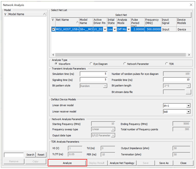
Figure 50.Waveform Viewer dialog opens providing all waveform for TX and RX.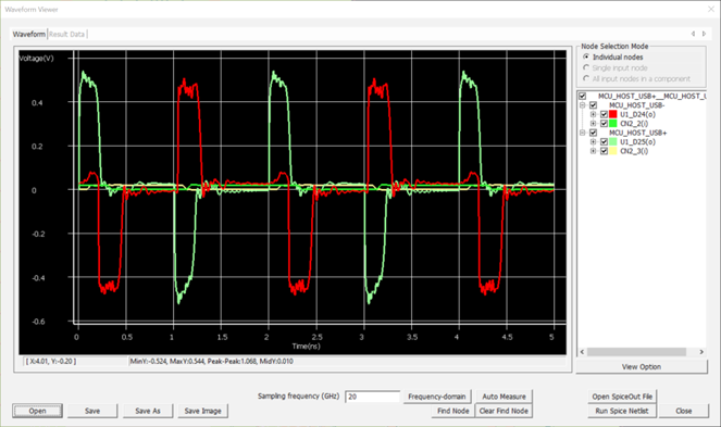
Figure 51. -
Uncheck the U1_D24(o) and
U1_D25(o) to check for RX waveform. Right click and
select Zoom all.
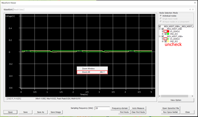
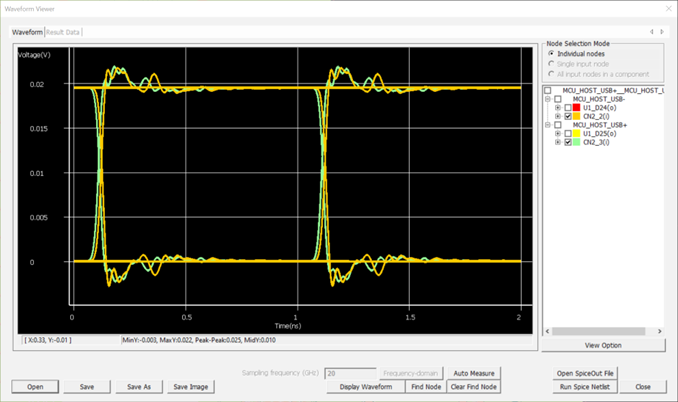
Figure 52.This will provide Waveform for RX.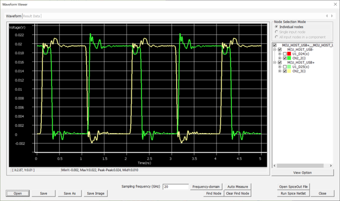
Figure 53. -
To check the impulse response, uncheck all waveform and select
IO_CN2_3.IMPULSE. Right click and select
Zoom all.
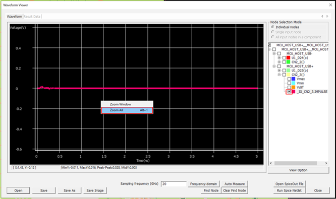
Figure 54.Waveform for Impulse response is displayed.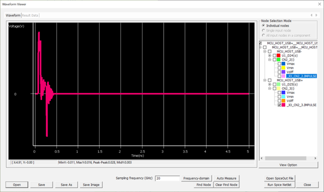
Figure 55.
Explore Eye Diagram Analysis
-
Select the desired net MCU_HOST_USB+ to analyze.
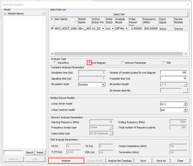
Figure 56.Waveform Viewer dialog displays. -
Select CN2_2(i) and CN_3(i) to
check the eye-diagram of output.