From the PollEx Launcher, Home ribbon, click the
PollExPCB icon.
From the menu bar, click File > Open and open the
PollEx_PCB_Sample_r<revision_number>.pdbb
file from
C:\ProgramData\altair\PollEx\<version>\Example\PollEx_PCB_Sample_r<revision_number>.pdbb.
From the menu bar, click File > Save As Project.
The Save As Project dialog opens.
In the Save As Project dialog, enter a new project name
and select the project folder to put in the design folder.
Click OK.
The project directory is created under the design folder.
PollEx_PCB_Sample_r<revision_number>.pdbb
and related files are copied to the project directory.
From the menu bar, click File > Exit.
Add New Dielectric Material
In this step, you will add a new dielectric material FR4.0 and PSR3.0.
From the menu bar, click File > Open and open the
PollEx_PCB_Sample_r<revision_number>.pdbb
file from
C:\ProgramData\altair\PollEx\<version>\Example.
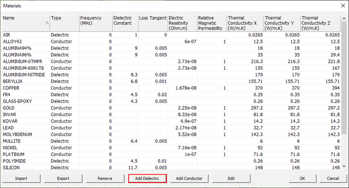
From the menu bar, click Properties > Material Library.
The Materials dialog opens.
Click Add Dielectric.
Figure 1.
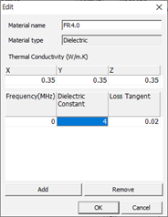
The Edit dialog opens.
Enter the following values and click OK.
For the Material name, enter FR4.0.
For X, Y, and Z, enter 0.35.
For Dielectric Constant, enter 4.0.
For Loss Tangent, enter 0.02.
Figure 2.
In the Materials dialog, click Add
Dielectric.
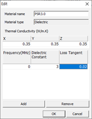
The Edit dialog opens.
Enter the following values and click OK.
For Material name, enter PSR3.0.
For X, Y, and Z, enter 0.35.
For Dielectric Constant, enter 3.0.
For Loss Tangent, enter 0.02.
Figure 3.
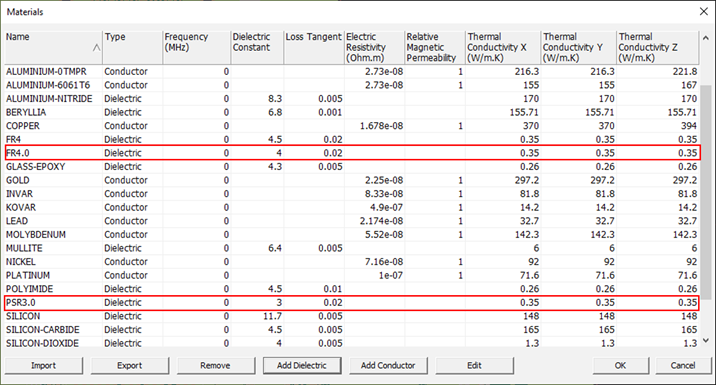
The FR4.0 and PSR3.0 materials are registered as new materials with the
names FR4.0 and PSR3.0. Figure 4.
Click OK to close the
Materials dialog.
Build PCB Stack
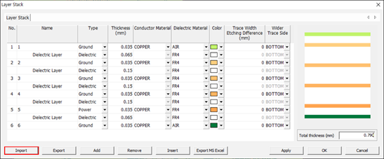
From the menu bar, click Properties > Layer Stack.
The Layer Stack dialog opens.
In the Layer Stack dialog, click
Import.
Figure 5.
Navigate to C:\temp\Altair-PollEx\PollExSI\Stackup, select
StandardStackup.udls, and click
Open.
PollEx provides a default stack-up, found here:
C:\ProgramData\altair\PollEx\<version>\Examples\Solver\SI\Stackup.
Change Dielectric Constant.
For the top layer, click and select
FR4.0.
For the bottom layer, click and select
FR4.0.
Figure 6.
The dielectric constant for the Top and Bottom layers is changed
from 4.5 to 4.0.
Add Solder resist layer to the Top and Bottom Layers.
Select the Top layer and click Insert.
The Add dialog displays.
In the Add dialog, select
PSR3.0 for the Dielectric material.
For Thickness, enter 0.02.
Figure 7.
Click OK.
The new Solder Resist layer is inserted at the top. Figure 8.
Select the Bottom layer and click Add.
The Add dialog displays.
In the Add dialog, select
PSR3.0 for the Dielectric material.
For Thickness, enter 0.02.
Figure 9.
Click OK.
The new Solder Resist layer is inserted at the bottom. Figure 10.
Click Export to save this stack-up.
Enter StandardStackup_PSR as the stack-up file name and
click Save.
Click OK.
Assign IBIS Model to Memory IC
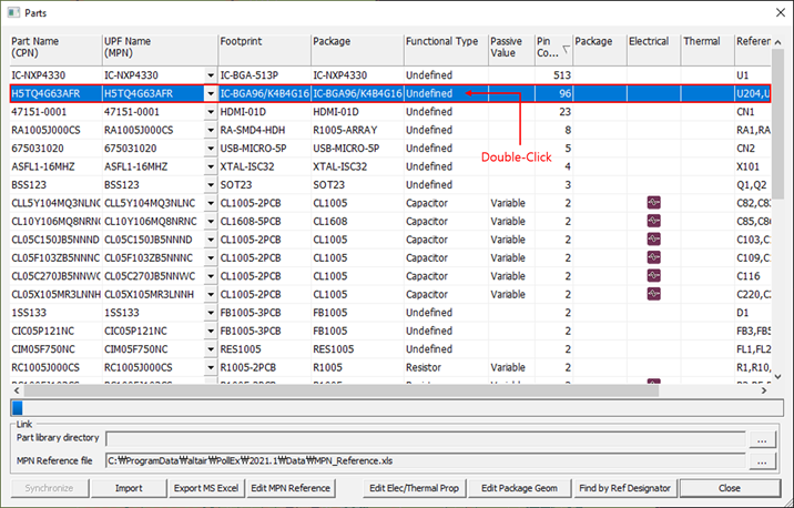
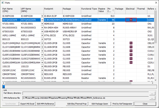
Click Properties > Parts.
The Parts dialog opens.
Double-click Pin Count to sort the results.
The passive component RLC values are automatically extracted from PDBB
data if the value property was correctly assigned in the PDBB database. Figure 11.
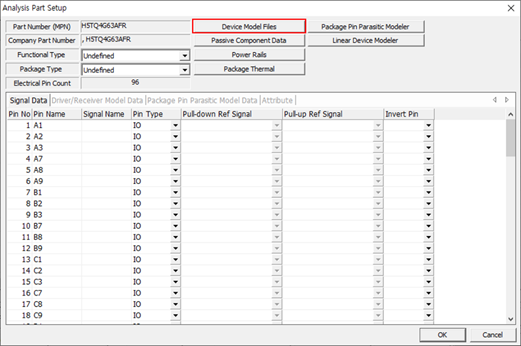
Double-click H5TQ4G63AFR.
The Electrical & Thermal Properties dialog
displays.
Click Device Model Files.
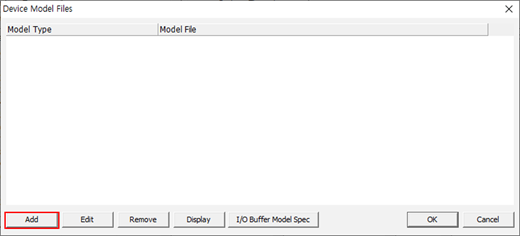
The Device Model Files dialog displays. Figure 12.
Click Add.
Figure 13.
Click to search and select the IBIS file
(C:\ProgramData\altair\PollEx\<version>\Examples\Solver\SI\Memory.ibs)
for DDR3 Memory device and click Open to open this file
and close this Explorer window.
Click OK to close the
Model Files dialog.
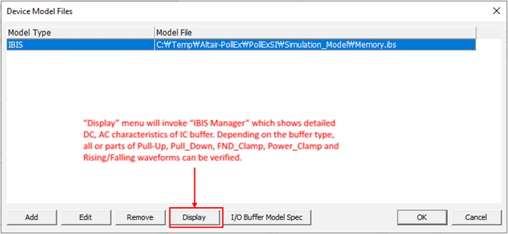
The Device Model Files dialog displays.
The full
location of the IBIS model file assigned to the DDR3 Memory device is shown
in the Device Model Files dialog. After selecting the
added IBIS file, the Display menu allows you to investigate the detailed
electrical properties of the Input/Output buffer models included in the IBIS
file.
Input buffer models only contain Power_Clamp and Ground_Clamp
characteristics. The DC (I-V) properties of Pull_Up and Pull_Down transistors
and AC properties given in Rising/Falling waveforms are just related to the
Output and IO buffer models.
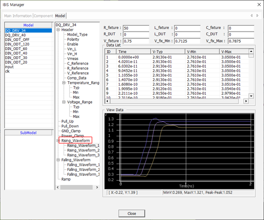
Select the first line and click Display to invoke the
IBIS Manager dialog.
Figure 14.
Click the Model tab and select
DQ_DRV_34 model from the list.
Find and review all of the AC/DC properties.
By exploring the buffer’s AC/DC characteristics, you can choose the proper
buffer model for SI Analysis. Figure 15.
Click Close to close the IBIS
Manager dialog.
To close the Device Model Files dialog, click
OK.
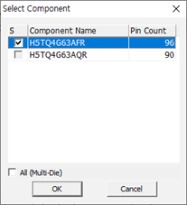
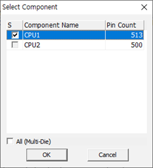
When the IBIS file contains numbers of different components (IC devices), you
need to select one of them. Pin count can be a good reference to select the
right one. In this case the Select Component dialog
opens.
Select the first component and click OK to close the Select Component
dialog.
Figure 16.
The Electrical & Thermal Properties dialog
opens.
The DDR3 device’s part properties are assigned automatically, as
shown in the Electrical & Thermal Properties
dialog. Figure 17.
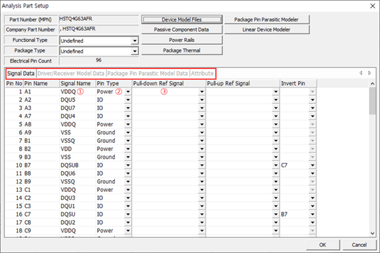
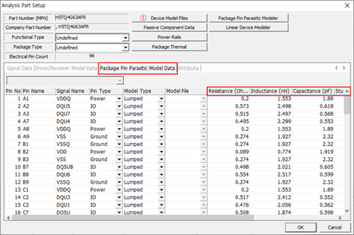
By selecting one of the tab menus among Signal Data,
Driver/Receiver Model Data, Package Pin Parasitic Model Data and Attribute,
detailed information displays.
The Signal Data tab menu shows basic
information such as Signal Name, Pin Type, Pull-down/Pull-up Ref Signal, and
Inverted Pin status. The Pin Type are None, Input, Output, IO, Terminator,
Power, Ground, NoConnect, TDI, TDO, TCK, TMS, and TRST.
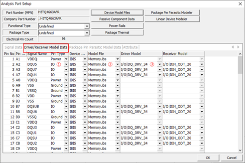
By selecting
the Driver/Receiver Model Data tab menu, you can verify the detailed
information related to I/O buffer assignment for each pin included in the IC
part.
Device Model column denoted as IBIS means that the pin’s model
is defined from IBIS data is not from SPICE, HSPICE or Linear Device Model.
As column, certain pins can select one from many available Driver or
Receiver models.
Figure 18. Figure 19.
Click OK to close the
Electrical & Thermal Properties dialog.
Click OK in the Device Model
Files dialog and select one of the proper components using pin count
information.
Select the first component and click OK to close the Select Component
dialog.
Figure 21.
Click OK to close the
Electrical & Thermal Properties dialog.
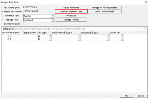
Assign Passive Component Data to R and C
Double-click RC1005J000CS in the
Parts dialog.
The Electrical & Thermal Properties dialog
displays.
Click Passive Component Data in the Electrical
& Thermal Properties dialog.
Figure 22.
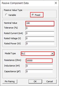
For Passive Value Type, select Fixed.
Leave the Model Type as RLC and enter the Nominal Value
and Resistance values.
Figure 23.
Click OK.
Click OK to close the
Electrical & Thermal Properties dialog.
Click Close to close the
Parts dialog.
Assign Passive Component Data
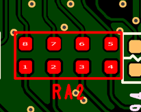
When a passive is an array component, you need to define
the pin pair configuration. Figure 24.
Click Properties > Parts.
The Parts dialog opens.
Double-click the RA1005J000CS part in the
Parts dialog.
Select Resistor as a function type and select
Chip resistor as a package type.
Click Passive Component Data in the Electrical
& Thermal Properties dialog.
Figure 25.
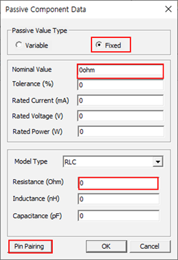
For Passive Value Type, select Fixed.
Leave the Model Type as the default RLC and enter the Nominal Value and
Resistance values as shown in Figure 26.
Figure 26.
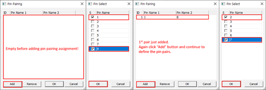
Click Pin Paring.
The Pin Paring dialog opens.
Each time Add is
clicked, the Pin Select dialog is newly displayed,
allowing you to set the next pin pair combination. The specified passive
component values will be assigned separately to these paired pins. Figure 27.
Click OK to close the
Pin Paring dialog.
Click OK to close the
Passive Component Data dialog.
Click OK to close the
Electrical & Thermal Properties dialog.
Click Close in the
Parts dialog to close it.
Assign Net Properties for Power
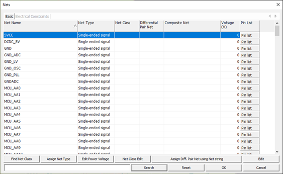
Click Properties > Nets.
The Nets dialog displays.
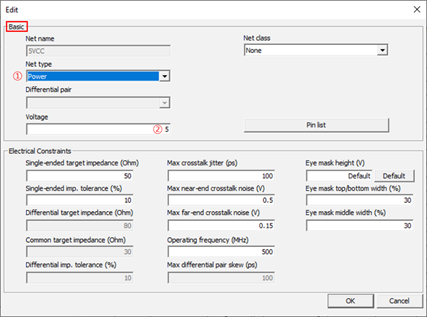
Double-click 5VCC.
The Edit dialog displays. Figure 28.
For Net Type, select Power.
For Voltage, enter 5.0.
Figure 29.
Click OK.
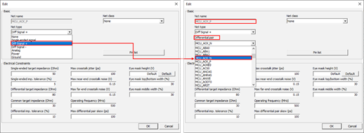
Assign Net Properties for Differential Pair
Double-click MCU_ACK_P net.
The Edit dialog displays.
Set the Net Type as Diff Signal +.
For Net type, select Diff Signal.
For Differential pair, select MCU_ACK_N.
Figure 30.
Click OK to close the
Edit dialog.
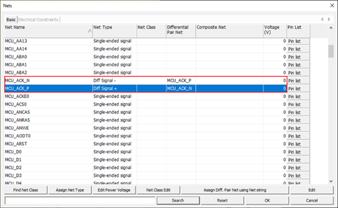
The MCU_ACK_P and MCU_ACK_N nets are combined as a differential pair
net.
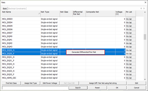
Select MCU_DQS0_N and MCU_DQS0_P
in the Nets dialog.
Figure 31.
Select Generate Differential Pair Net from the context menu.
Figure 32.
The Edit dialog opens.
Click OK to close the
Edit dialog.
Click OK to close the
Nets dialog.
Assign Net Properties Automatically
Click Properties > Nets.
The Nets dialog displays.
Click Assign Net Type.
PollEx automatically assigns the Net Type of all
nets using the information in the IBIS model and net name string. Figure 33.
Click Find Net Class.
PollEx automatically assigns the Net Class to all nets
using pre-defined Net Class Definition. When creating a Net class, if there is a
net with duplicate definitions, the following dialog opens. Figure 34.
Click OK.
In this case, you have to select the Net class of the corresponding nets.
Since the Net Class of both VCC1P0_LVDS net and VCC1P8_LVDS net is Power. Figure 35.
Click OK to close the
Nets dialog.
Create Composite Net
Click Properties > Composite Nets.
In the composite component section region, check
Resistor and Capacitor.
Click Generate Composite Net.
The Selects Nets to Exclude dialog opens.You can
specify nets that should not be composited with other nets, such as Power and
Ground nets.
Click OK and check the listed
composited nets.
Figure 36.
Click Composite Data or Pin List
to review composite net structure or the pin list.
Figure 37.
If you want to check the total net composition status for the composited
nets, use the Option > Net 2D/3D Viewer menu. Select the composite net
CN-||MCU_HDMI_HPD||SIGN00248||. The entire structure
of the composite net is displayed in the left window.
Extract the Transmission Line Properties
In this step, you will extract the transmission line properties of specified
geometry.
Click Properties > Layer Stack.
The Layer Stack dialog opens.
Execute the Import menu.
The Explorer dialog opens.
Select the stackup file to be used from
C:\ProgramData\altair\PollEx\<version>\Examples\Solver\SI\Stackup.
Select StandardStackup.udls for 6-layer stack-up.
Click Open to select this stackup.
Click OK to close the
Layer Stack dialog.
Click File > Save to save the current environment to PDBB file.
Click Analysis > Signal Integrity > Transmission Line Analysis.
The Transmission Line Analysis dialog
opens.
Enter the model name as CLOCK_Diff.
Click Extract Trace Parasitic Parameters.
Click Add Conductor.
Figure 38.
The Conductor Information dialog
displays.
Enter 0.1 for the Width and click OK.
Figure 39.
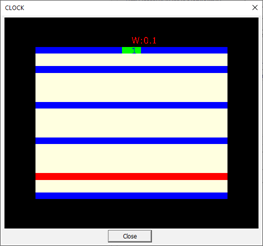
Click Display Model.
Review the PCB stackup structure and close the dialog.
Figure 40.
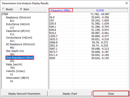
Click Analyze.
The Transmission Line Analysis-Display Results
dialog opens. The default properties shown are Char-Impedance.
Switch the property display by clicking other characteristics.
Figure 41.
Click Close to close the Transmission Line
Analysis-Display Results dialog.
By adding one more line, you can configure and analyze the electrical
properties for differential pairs.
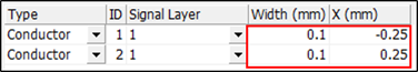
Click Add Conductor.
Enter 0.1 for Width.
Enter 0.2 for X.
Click OK.
X stands for the center-to-center distance between two traces.
Figure 42.
Figure 43.
Click Display Model.
Review the PCB stackup structure and close the dialog.
Two traces will be located at the same signal layer numbered as 1 and 2. Figure 44.
Click Analyze.
The Transmission Line Analysis-Display Results
dialog opens. The default properties shown are Diff-Impedance. Switch the
property display by clicking other characteristics. Figure 45.
Click Close to close the Transmission Line
Analysis-Display Results dialog.
Click Save and check this transmission line model shown
in the Model Name area of the Transmission Line Analysis
dialog.
Figure 46.
To use the saved model later, click the CLOCK_Diff
model, and click Copy.
The parameters stored in this model are copied to the right window. Figure 47.
Model Routed Trace.
Click Generate Multiple Models.
The Generate Multiple Models dialog
displays.
Click Model Routed Trace to extract the current
PCB trace model.
Click Assign Model Names to assign the default
model name to extracted trace models.
Figure 48.
Click OK to close
this dialog and check these transmission line models shown in the Model
Name area in the Transmission Line Analysis
dialog.
Figure 49.
Select all of the transmission line models and click Run
Analysis to analyze them.
Enable the checkboxes of all the Impedance and Delay items.
Figure 50.
Click Close.
Get Impedance Matching Trace
Click Analysis > Signal Integrity > Transmission Line Analysis.
The Transmission Line Analysis dialog
opens.
Enter CLOCK_DIFF_100 for the model name.
Click Get Impedance Matching Trace.
Change the Signal type to Differential narrow.
Change the Unknown property to Separation.
Enter 0.1 for the Trace width and
100 for Differential impedance and click
Analyze.
Figure 51.
Check the calculated Diff-Impedance value in the Transmission Line
Analysis-Display Results dialog.
Click Close to close the Transmission Line
Analysis-Display Result dialog.
When the target impedance 100 is achieved, the center-to-center distance X
displays. The edge to edge distance is 0.4.
Click Display Model.
The structure is shown. Figure 52.
Click Save and Close to close the
dialog.
Explore the Waveform Analysis
Select Analysis > Signal Integrity > Network Analysis.
The Network Analysis dialog opens.
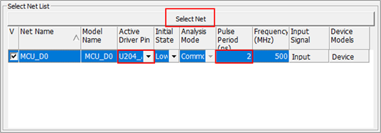
Click Select Net.
Select MCU_D0 and click OK.
Enable the MCU_D0 checkbox.
Figure 53.
Click and select U204-A2.
By setting the Active Driver Pin, you can determine the driving direction of
the MCU_D0 net. U204 is the reference name of a DDR memory device. This setting
represents the Data Read mode. For bidirectional signals, both directions must
be analyzed. You can select the analysis direction by setting the Active Driver
Pin. For example, if it is set to U204_A2, the direction of data transfer from
Memory to CPU, that is, read cycle analysis.
Change the Pulse Period from 2 to 1.25.
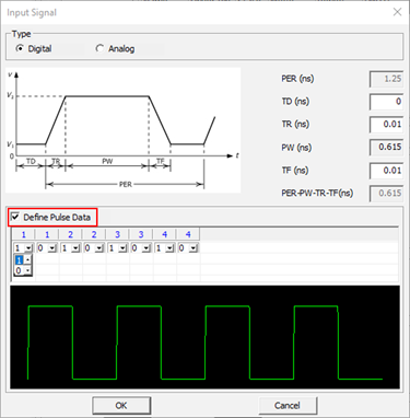
Click Input Signal to verify the device pin model’s
switching characteristics.
Total Pulse Period: (1.25) ns = TR (0.1) + 2 * PW (0.525) + TF (0.1). TD means
it adds the specified time as latency of the excitation. 1.25ns pulse will be
applied just after the TD (ns) pauses.
Enable the Define Pulse Data checkbox to specify the
switching format.
Figure 54.
Click OK to close the
Input Signal dialog.
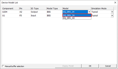
Click Device in the Network
Analysis dialog.
Check the connected components and pins to the selected net using the
Device Model List dialog.
You can change the actual driver pin model among selectable models.
For the U204 component, select DQ_DRV_34 for the
model.
Figure 55.
For the U1 component, select ODT_120 for the model and
click OK.
The default signaling time is set by 5ns, then four cycles of the switching
signals will be applied during the SPICE waveform analysis.
Select Waveform as an Analysis Type field.
Click Analyze.
When the waveform analysis starts, electromagnetic simulation extracts the
SPICE model for the selected net. The excitation source signal is applied to the
net which is specified by the assigned pin model’s operating characteristics and
the values defined at Input Signal and Pulse Period. When the simulation is
done, the Waveform Viewer opens or exploring the waveforms.
Click View Option to open the View
Option dialog.
Close the View Option dialog.
Close the Waveform Viewer.
Click Save to save the simulation result.
The nets are saved.
Explore Eye Diagram Analysis
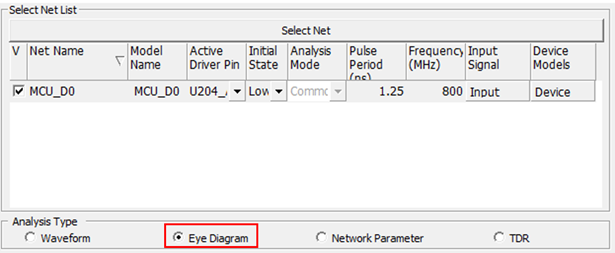
For Analysis Type, select Eye Diagram.
Select the desired net MCU_D0 to analyze.
Figure 56.
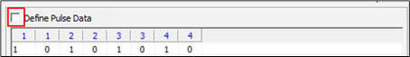
Click the Input Signal column to open the
Input Signal dialog.
Disable the Define Pulse Data checkbox.
Figure 57.
Click OK to close the
Input Signal dialog.
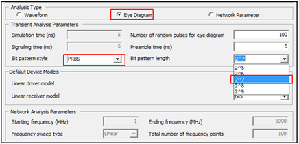
Select Eye Diagram as an Analysis Type.
Change the Bit pattern style to PRBS and the Bit pattern
length to 2^7.
Figure 58.
Click Analyze.
All 2^7 numbers of random bit will be applied to the net; the detailed bit
signal pattern will follow the shape defined at Input Signal.
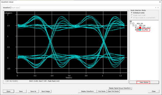
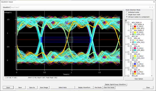
The Waveform Viewer dialog displays.
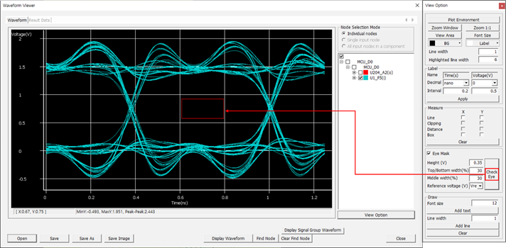
Select U1_F5(i).
Click View Option to open the View
Option dialog.
Figure 59.
Change the value of the Eye Mask region and click Check
Eye.
The Eye mask opens.
Move the cursor and click the position where you want to check.
Figure 60.
Close the Waveform Viewer dialog.
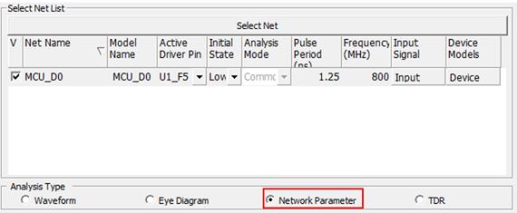
Explore the Network Parameter Analysis
Select the Analysis Type as Network Parameter, which
enables the S, Y, Z-Parameter extraction to the selected net(s).
Figure 61.
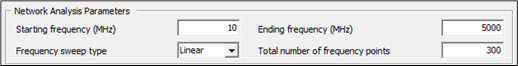
Leave the default values for the analysis.
300 frequency points are used for the parameter’s extraction. Figure 62.
Click Analyze to start the analysis.
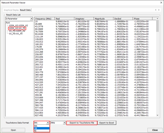
Click Result Data, to verify the extracted parameters in
table data format.
Figure 63.
Select U204_A2::U1_F5.
The appropriate values display. By selecting one of the Touchstone data
formats , you can export the data in Touchstone and Excel formats.
Select DB as the Touchstone Data Format.
Click Export to Touchstone File menu to save the result
s-parameter file.
Click Save and Close to close all
dialogs.
Click Close to close the Network
Analysis dialog.
Extract the Spice Net List
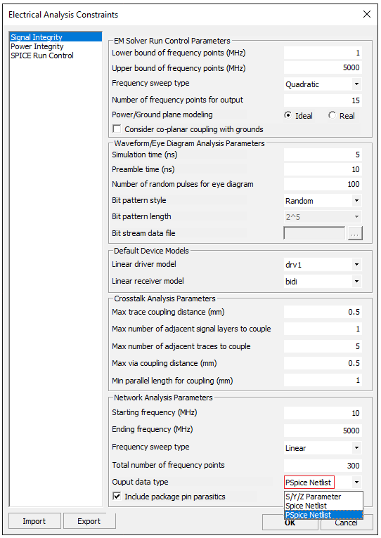
Execute Analysis > Signal Integrity > Electrical Analysis Constraints.
The Environment dialog opens.
Select PSpice Netlist as an Output data type and click
OK.
Figure 64.
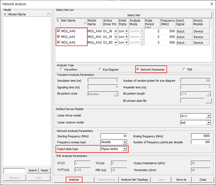
Click Analysis > Signal Integrity > Network Analysis.
The Network Analysis dialog opens.
Select the target nets to extract the Spice net list.
Select the Network Parameter as an Analysis type.
You can also select Output data type in this dialog.
Click Analyze to extract the Spice Net List.
When the simulation is done, the Explorer window opens to designate the
folder to save the Spice Net Lists. Figure 65.
Set the folder path and click OK to save the results.
The default path is the Signal Integrity directory of the current project. The
*.lib files are created in the designated
folder.
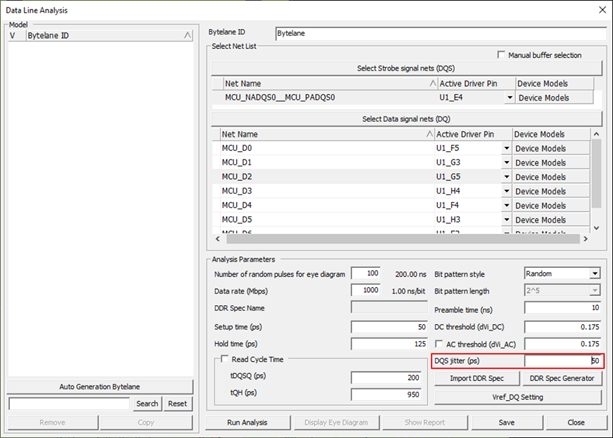
Explore Data Line Analysis
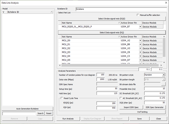
Click Analysis > Signal Integrity > Data Line Analysis.
Select required nets manually.
Click the Select Strobe signal nets tab in the
Data Line Analysis dialog.
Select MCU_DQS0_N differential pair nets and
click OK.
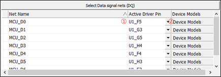
Click Select Data signal nets.
Select MCU_D0~MCU_D7 and click
OK.
Figure 66. Figure 67.
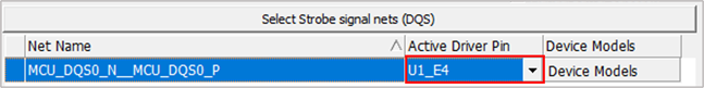
Click and select
U1_E4.
For bidirectional signals, both directions must be analyzed. You can
select the analysis direction by setting the Active Driver Pin. For
example, if it is set to U1_E4, the direction of data transfer from CPU
to Memory, that is, write cycle analysis.
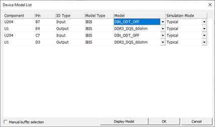
Click Device Models.
You can check the connected components and pins to the selected net in
the Device Model List dialog. You can change the
actual driver pin model among selectable models, if needed.
For U204, select DIN_ODT_OFF for the model and
click OK.
Figure 68.
For MCU_D0~MCU_D7 nets, click and select
U1_F5.
Figure 69.
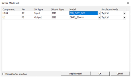
Click Device Models.
You can check the connected components and pins to the selected net
using the Device Model List dialog. You can change
the actual driver pin model among selectable models, if needed.
For U204, select DIN_ODT_OFF for model and click
OK.
The rest of data byte nets driver configuration will be changed
automatically with the same configuration of MCU_D0 net. Figure 70.
Set the DQS Jitter value to 50 in the Analysis
Parameter section.
Figure 71.
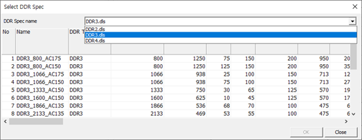
Click Import DDR Spec.
You can select the required DDR operating speed.
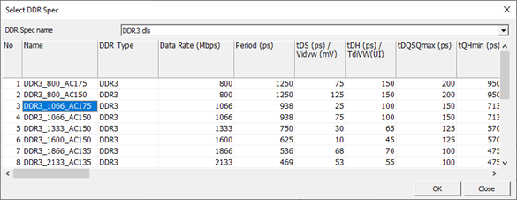
Select DDR3.dls for a DDR Spec name field.
Figure 72.
Set the Data Rate to 1066 for DDR3_1066_AC175
and click OK.
Figure 73.
Click Run Analysis.
When the data line analysis starts, electromagnetic simulation
extracts the SPICE model for the selected net. The excitation source
signal is applied to the net which is specified by the assigned pin
model’s operating characteristics. When the simulation is done, the
Waveform Viewer dialog displays for exploring
the signal's waveforms. Figure 74.
The eye-mask for DDR3_1066_AC175 operation also
displays.
Close the Waveform Viewer dialog.
Click Save to save the result.
Select required net group automatically.
Select Analysis > Signal Integrity > Data Line Analysis.
Click Auto Generation Bytelane to extract
possible byte lane combinations automatically.
Figure 75.
Select the required combination and click
copy.
Selected combinations are copied. Figure 76.
Click Close to close the Data Line
Analysis dialog.
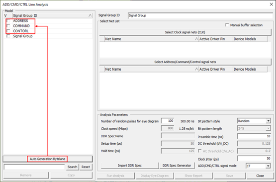
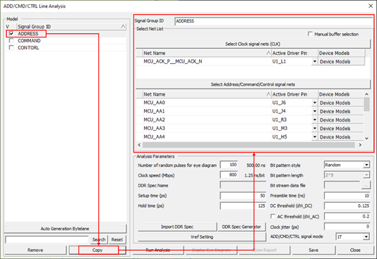
Explore ADD/CMD/CTRL Line Analysis
Click Analysis > Signal Integrity > ADD/CMD/CTRL Line Analysis.
Select required nets manually.
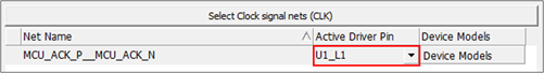
Click Select Clock signal nets in the the
ADD/CMD/CTRL Line Analysis dialog.
Select MCU_ACK_P differential pair nets and
click OK.
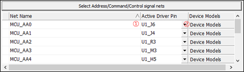
Click Select Address/Command/Control signal
nets.
Select MCU_AA0~MCU_AA14 and click
OK.
Click and select
U1_L2.
Figure 77.
Only the CPU can drive clock and control line at DDR bus.
Click Device Models in the
ADD/CMD/CTRL Line Analysis dialog.
You can check the connected components and pins to the selected net in
the Device Model List dialog. You can change the
actual driver pin model among selectable models, if needed.
Figure 79.
Only the CPU can drive clock and control line at DDR bus. The rest
of address nets driver configuration will be changed automatically with
the same configuration of MCU_AA0 net.
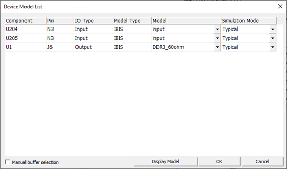
Click Device Models in the Select
Address/Command/Control signal nets dialog.
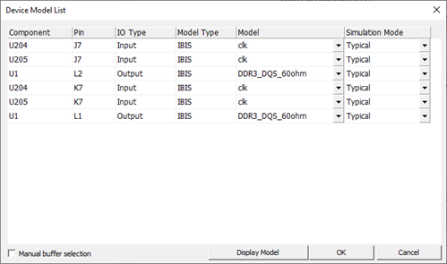
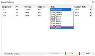
For U204 and U205, select input for model.
For U1, select DDR3_60ohm for model and click
OK.
The rest of address nets driver configuration will be changed
automatically with the same configuration of MCU_AA0 net. Figure 80.
Set the Clock Jitter value to 50.
Set the ADD/CMD/CTRL signal mode to 1T.
Click Import DDR Spec.
You can select the required DDR operating speed.
Select DDR3.dls for a DDR Spec name field.
Figure 81.
Select the Data Rate as 1066 for DDR3_1066_AC175
and click OK.
Figure 82.
Click Run Analysis.
When the address/command/control line analysis starts, electromagnetic
simulation extracts the SPICE model for the selected net. The excitation
source signal will be applied to the net which is specified by the
assigned pin model’s operating characteristics. When the simulation is
done, the Waveform Viewer dialog opens for
exploring the signals waveforms. The eye-mask for DDR3_1066_AC175
operation is also displayed.
Close the Waveform Viewer dialog.
Click Save to save the results.
Select required net group automatically.
Click Auto Generation Bytelane to extract
possible address/control/command line combinations automatically.
The result combination displays in the Model window. Figure 83.
Select the required combination and click
Copy.
The selected combinations are copied. Figure 84.
Click Close to close the ADD/CMD/CTRL Line
Analysis dialog.
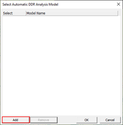
Explore Automatic DDR Bus Analysis
Select Analysis > Signal Integrity > Automatic DDR Bus Analysis.
The Select Automatic DDR Analysis Model dialog
displays.
Click Add to create a new model.
Figure 85.
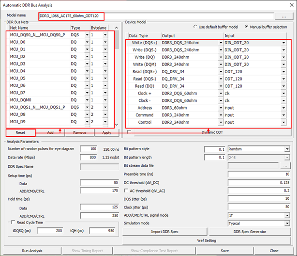
The Automatic DDR Bus Analysis dialog
displays.
Enter the Model name as DDR3_1066_AC175_60ohm_ODT120 and
click Reset.
Figure 86.
Under the DDR Bus Nets section, all automatically extracted DQS, DQ, CLK,
ADD, CMD, and CTRL nets are listed.
Review the extracted net names.
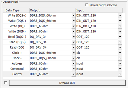
In the Device Model section, select output and input models as shown in
.
Figure 87.
Click Import DDR Spec and select
DDR3.dls for the DDR Spec name field.
Figure 88.
Set the Data Rate to 1066 for DDR3_1066_AC175 and click
OK.
Figure 89.
Set the DQS Jitter value to 50 in the Analysis Parameter
section.
Set the Clock Jitter value to 50 in the Analysis
Parameter section.
Set the ADD/CMD/CTRL signal mode value to 1T
in the Analysis Parameter section.
Enable the AC threshold(dvi_AC) checkbox in the Analysis Parameter
section.
Click Save.
The Automatic DDR Bus Analysis is ready.
Click Run Analysis.
Data line analysis and ADD/CMD/CTRL line analysis models are automatically
constructed, and analyses are automatically performed on all of the
models.
The analysis results are automatically saved. The eye diagrams and timing
margins of individual data line analysis and ADD/CMD/CTRL line analysis
models can be viewed in Data Line Analysis and ADD/CMD/CTRL Line Analysis,
respectively.
The automatic DDR bus analysis models with analysis results are saved in the
DDR directory under Signal_Integrity of the PCB design project folder.
DDR3_1066_AC175_60ohm_ODT120.DBM is used for the
file name.
When the automatic DDR Bus analysis starts, all options at the bottom of the
Automatic DDR Bus Analysis dialog are invisible,
and the progress bar appears. The electromagnetic simulation extracts the
SPICE model for the selected net. The excitation source signal is applied to
the net which is specified by the assigned pin model’s operating
characteristics. When the simulation is done, all of the options at the
bottom of the Automatic DDR Bus Analysis dialog are
visible.
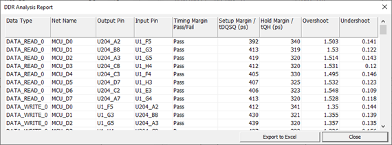
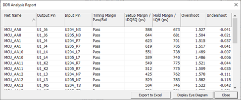
Click Show Timing Report.
The setup and hold margin of all signals displays. Figure 90.
Click Close to close the DDR Analysis
Report dialog.
Click Close to close the Automatic DDR Bus
Analysis dialog.
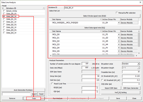
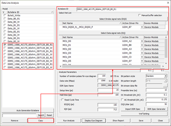
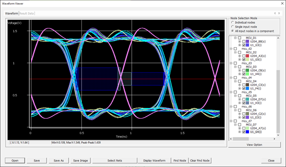
Review data line analysis result.
Select Analysis > Signal Integrity > Data Line Analysis to review data bus analysis results.
Select DDR3_1066_AC175_60ohm_ODT120_B0_R1.
Click Copy.
Figure 91.
Click Display Eye Diagram to review the Eye
Diagram.
Figure 92.
Click Close to close the Waveform
Viewer dialog.
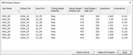
Click Show Report to review timing margin.
Figure 93.
Click Close to close the dialog.
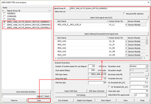
Review Address, Command, and Control line analysis result.
Select Analysis > Signal Integrity > ADD/CMD/CNTR Line Analysis to review ADD/CMD/CTRL line analysis results.
Select
DDR3_1066_AC175_60ohm_ODT120_ADDRESS1.
Click Copy.
Figure 94.
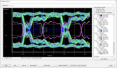
Click Display Eye Diagram to review the Eye
Diagram, then close it.
Figure 95.
Click Show Report to review timing margin, then
close it.
Figure 96.
Close the ADD/CMD/CTRL Line Analysis dialog.
Explore Crosstalk Analysis
Click Properties > Layer Stack.
The Layer Stack dialog opens.
Execute the Import menu.
The Explorer dialog opens.
Find the directory path in which your own stack-up files in navigation tree
section: C:\temp\Altair-PollEx\PollExSI\Stackup.
Select StandardStackup2.udls for 6-layer stack-up.
Close the Layer Stack dialog.
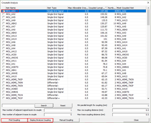
Select Analysis > Signal Integrity > Crosstalk Analysis.
Click Find Coupling.
The MCU_AA3 net has the longest coupling length.
Select MCU_AA3.
Figure 97.
Click Display/Analyze Coupling.
The Display/Analyze Coupling dialog
displays.
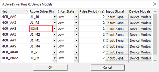
Click Active Driver Pins & Device Models to open the
dialog.
You can define whether the excitation signal is applied or not for each
aggressor net.
If the Active Driver pin item is selected as NONE, the
corresponding net maintains a steady state without applying a stimulus
signal during crosstalk analysis.
Click OK.
Figure 98.
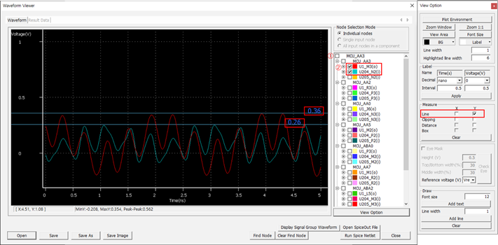
Click Run Analysis to start crosstalk analysis.
The Crosstalk Analysis runs and the Waveform Viewer
dialog opens.
Click V to hide all waveforms.
Select UI_M3(o) and U204_N2(i),
to display the victim net’s coupled noise waveform. (Near End Crosstalk)
Using the measure function, you can find the peak to peak coupled NEXT noise
level reaching to about 0.36V and FEXT noise level reaching to about
0.26V.
Figure 99.
Close all Crosstalk Analysis related dialogs.
Reduce Crosstalk Noise
In this step, you will reduce crosstalk noise by shortening the plane
distance.
There are many ways to reduce crosstalk noise:
Reduce coupling length.
Increase the separation between the two nets.
Reduce the height of the signal line and reference plane.
In this step, you will apply the third method.
Click Properties > Layer Stack.
Change the thickness of the dielectric layer to 0.065
between Top and Inner_Layer_2.
Change the thickness of the dielectric layer to 0.065
between Bot and Inner_Layer_5.
Click OK to close the
Layer Stackup dialog.
Figure 100.
Select Analysis > Signal Integrity > Crosstalk Analysis.
Click Find Coupling.
Select MCU_AA3.
Click Display/Analyze Coupling.
Click Run Analysis in the Display/Analyze
Coupling dialog.
Select MCU_AA3.
You can verify that having closely placed ground plane to the signal plane
reduces the crosstalk noise dramatically. Using the measure function, you can
find the peak to peak coupled NEXT noise level reduced to about 0.22V and FEXT
noise level reduced to about 0.20V. Figure 101.
Close Waveform Viewer related dialogs.
Extract Network Parameter
In this step, you will extract network parameter among coupled net
groups.
When you change the Analysis Type in the Display/Analyze Coupling dialog from
Waveform to Network Parameter. You can have S, Y and Z-parameters for all ports
which are assigned at the driving and receiving ends of all victim and aggressor
nets.
Click Network Parameter as the Analysis
Type.
Click Run Analysis.
Figure 102.
Explore the extracted S, Y, Z parameters in Graphical or table format.
The touchstone file can also be exported.
Close all Crosstalk Analysis related dialogs.
Analyze Single-Ended Topology
From the menu bar, click Analysis > Signal Integrity > Net Topology Analysis > Net Topology Analyzer.
From the menu bar, click File > New.
Enter Clock for Model Name and click OK.
Select Type 5, which has parallel ac termination, and
click Close.
Figure 103. Figure 104.
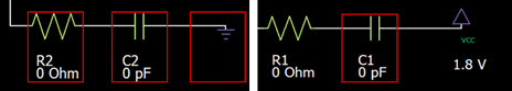
Select R2, C2, and
GND and click delete.
All three elements are removed. Figure 105.
Click C1 and Delete.
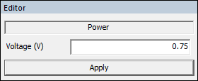
Click VCC, assign the Voltage from 1.8 V to
0.75V as a termination voltage and click
Apply.
Figure 106.
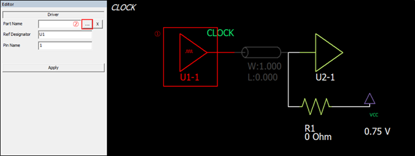
Click U1-1 and click Part
Name.
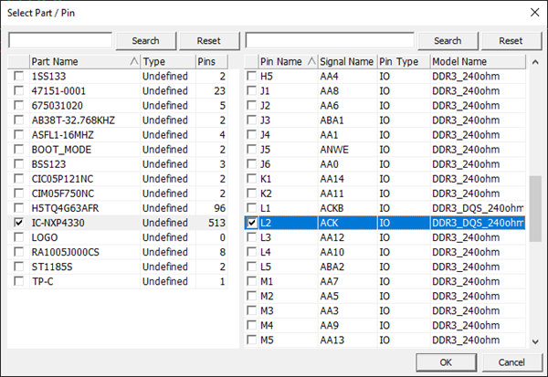
Figure 107.
Select IC-NXP4330 and select the L2 pin ACK.
The buffer model DDR3_DQS_60 ohm which connected to the L2 pin of IC-NXP4330
is used.
Click OK.
Figure 108.
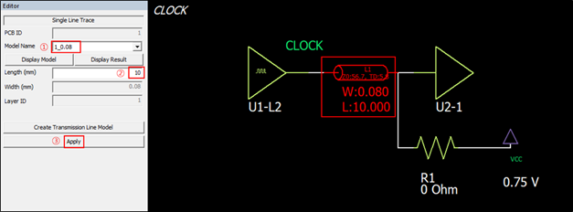
Click single line TML model and select one of the trace models.
The selected 1_0.08 model denotes that it is routed at 1 layer having 0.08
(mm) width. The thickness of the trace and distance to the ground will follow
the stack up information.
Enter 10 as the length.
Click Apply.
Figure 109.
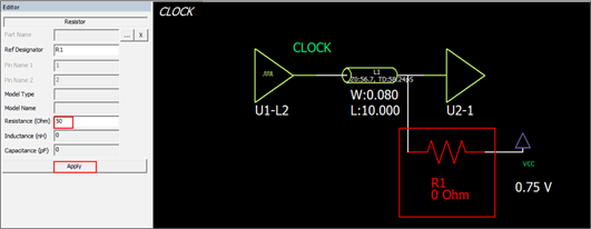
Click R1.
You can select a resister from the activated PCB system, or enter the value as
50ohm and click Apply. Figure 110.
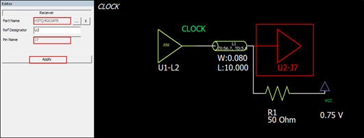
Click U2-1 and then click Part
Name.
Select and assign Receiver (U2-1) and click Apply.
The Part Name is H5TQ4G63AFR and the Pin Name is J7.
Click OK.
Figure 111.
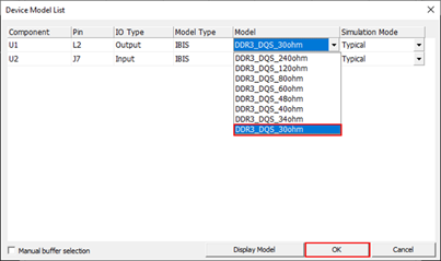
From the menu bar, click Analysis > Network Analysis.
The Topology Network Analysis dialog displays for
detailed simulation setup.
Click Device Models and then select the
DDR3_DQS_30ohm.
Click OK.
Figure 112.
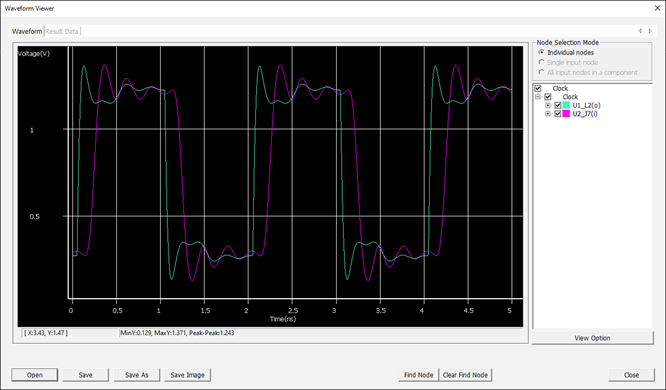
Click Analyze.
The simulated waveform is shown.
From the menu bar, click File > Save As to save and use the waveform at a later time.
Figure 113.
Close all dialogs related to the topology analyzer.
Analyze Topology
In this step, you will analyze topology from selected netlist.
From the menu bar, click Property > Layer Stack.
The Layer Stack Manager dialog
displays.
Execute the Import menu.
The Explorer dialog displays.
Find the directory path for your stack-up files in the navigation tree section:
C:\ProgramData\altair\<version>\Examples\Solver\SI\Stackup.
Select StandardStackup.udls for 6-layer stack-up.
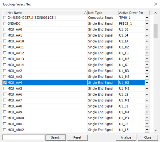
From the menu bar, click Analysis > Signal Integrity > Net Topology Analysis > Select Net for Analysis.
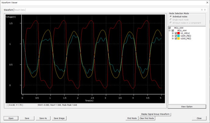
Figure 114.
Select MCU_AA4 and click
Analyze.
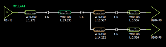
The lengths from driver to two receivers are slightly different among others.
This means that all receivers are taking signals from driver through different
electrical lengths. Therefore, there might be significant differences for the
receiving signals between two DDRs. Figure 115.
The Net Topology Analyzer dialog
opens.
From the menu bar, click Analysis > Network Analysis for the waveform analysis setup.
Click Waveform for the Analysis Type.
Change the Pulse Period from 2 (ns) to 1.0 (ns) and
extend both Simulation time (ns) and Signaling time (ns) as 5.
Click Device Models, select the
DDR3_30ohm model in U1, and click OK.
Figure 116.
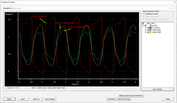
Click Analyze to start the simulation.
Figure 117.
Click Save As in the Waveform Viewer and save the
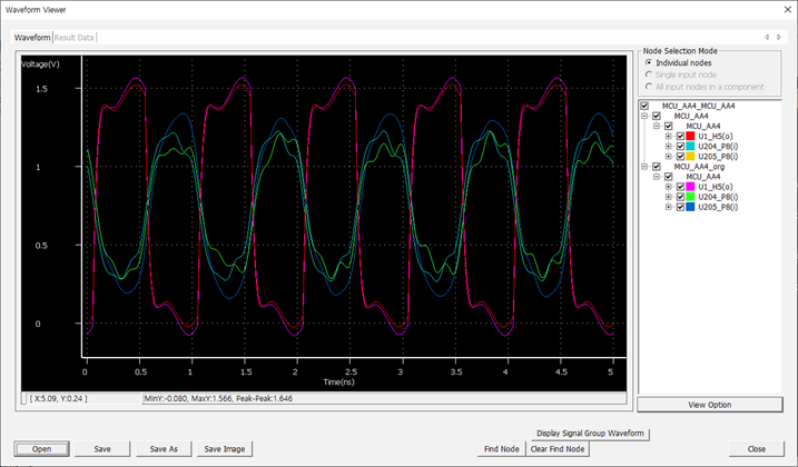
waveform name as MCU_AA4_org.spw.
Close the Waveform Viewer.
The original net waveform will be compared later with the modified topology.
This activated PCB system is not an actual working system but is designed
partially only for demonstration purpose. Therefore, the timing information and
signal levels might not be adaptive to the technical standard related to the
devices employed in this demo PCB. Figure 118.
The total 5 pulse sequences are shown in the Waveform Viewer. The
receiving signals show big deviation.
Generally, the lengths for the
net segments that are close to the driver should be longer than the other
ones routed further away from the driver. The total path (electrical) length
to each receiver from the driver should be the same.
Therefore, at
next trial, you will adjust net lengths as the same for all and route it
over the same layer. Vias will be removed, and the parallel termination will
be applied at the first T-branch location for expecting better receiving
signals.
Click Close to close the Waveform
Viewer dialog.
Click Close to close the Topology Network
Analysis dialog.
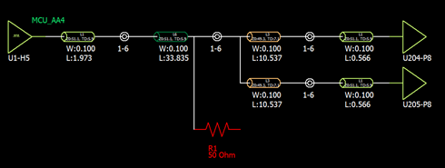
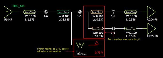
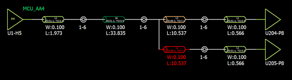
Change Length 3rd branch for U205 models to
10.537.
Click Apply.
Figure 119.
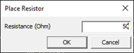
Click Resistor and enter 50 for the
resistance value.
Click OK.
The mouse cursor opens with the resistor symbol.
Move the mouse cursor over 1st net trace connected to the driver, press the
Ctrl key, and click the
1st net.
Press Esc to exit the resistor
insertion mode.
The resistor is added at parallel to the clicked 1st net elements. Figure 120. Figure 121.
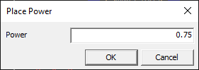
Select Edit > Add > Power to add DC voltage source to the net.
Enter 0.75 V and click OK.
Click R1.
Press Esc.
Figure 122.
Final Topology for Analysis.
Figure 123.
From the menu bar, click Analysis > Network Analysis, change the Pulse Period from 2 (ns) to 1.0 (ns) and
extend both Simulation time (ns) and Signaling time (ns) to 5.
Click Device Models and select the
DDR3_30ohm model in U1.
Click OK.
Click Analyze to start the simulation.
Figure 124.
Click Open and select the original net waveform
MCU_AA4_org.spw.
Click No.
Figure 125.
Explore Radiated Emission Analysis
Run Radiated Emission Analysis.
Execute the Analysis-Radiated Emission
menu.
The Radiated Emission Analysis dialog
opens.
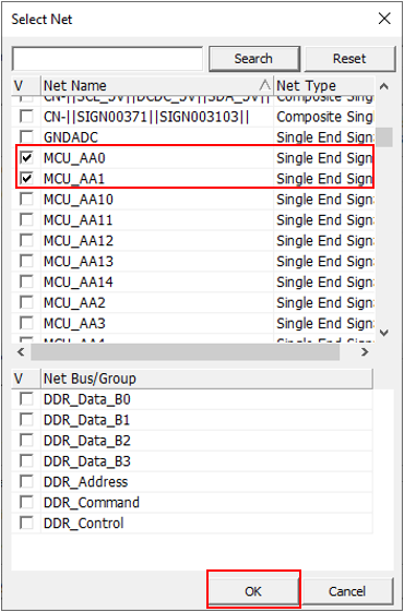
Click Select Net.
The Select Net dialog opens.
Multi select MCU_ACK, MCU_ACKB,
MCU_AA0, MCU_AA1, and
click OK to close the
dialog.
Figure 126.
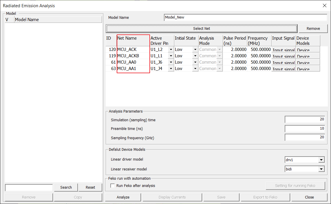
In the Radiated Emission Analysis dialog, enter
DDR_Address for the Model Name.
Click Analyze to start Radiated Emission
Analysis.
Click OK.
Click Save to save the result.
The model name is listed. Figure 127.
Review the analysis result of selected nets.
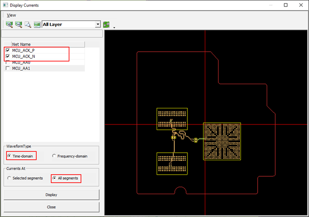
Click Display Currents to review the
result.
You can review the current waveform of the selected net or selected
segment in time domain and frequency domain.
The Display Currents dialog
opens.
Select MCU_ACK(MCU_ACK_N) and
MCU_ACKB(MCU_ACK_P) in the Net Name
field.
Select Time-domain.
The time-domain current waveform shows.
Select All segments to how the current waveform
of the selected nets.
Figure 128.
Click Display.
You can review the current waveform of the start point and the end
point of each segment. You can measure the time and amplitude by
clicking View Option.
The Radiated Emission Time-Domain Viewer
dialog opens.
Click Close to close the dialog.
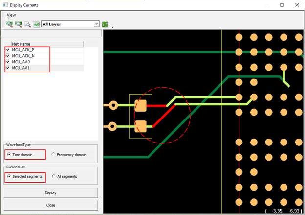
Review the analysis result of selected segment.
Select all nets in the Net Name field.
For Waveform Type, select Time-domain.
The time-domain current waveform shows.
Select Currents At as Selected segments.
The current waveform of selected segments shows.
Click the required segment to review the results.
Figure 129.
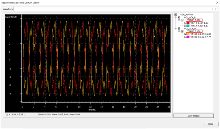
Click Display.
The Radiated Emission Time-Domain Viewer
dialog opens. You can review the current waveform of the start point and
end point of the selected segments. Figure 130.
Click Close to close the dialog.
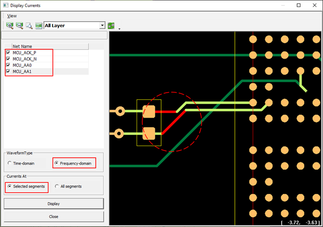
Review the frequency-domain analysis result of selected segment.
Select all nets in the Net Name field.
For Waveform Type, select
Frequency-domain.
The time-domain current waveform shows.
Select Currents At as Selected segments.
The current waveform of selected segments shows.
Click the required segment to review the results.
Tip: Press Ctrl to select multiple
segments.
Figure 131.
Click Display.
The harmonic frequency of the current of the selected net is
displayed. The current magnitude values among ports are initially
displayed. You can change the segment port pair selections and change
the plot type to decibel, phase, real number, or imaginary number. Also,
you can choose the scale of frequency axis or value axis. Many display
and measurement options are available in the Frequency-Domain
Viewer.
The Radiated Emission Frequency-Domain
Viewer dialog opens.
Click Close to close the Radiated
Emission Frequency-Domain dialog.
Click Close to close the Display
Currents dialog.
Export result in XML format.
Click Export to Feko to save the analysis result
in XML format.
This file is saved in the
Radiation/Model_Name directory under the PCB
design job folder. The model name and .REI is used
for the file name.
 and select
FR4.0.
and select
FR4.0.

 to search and select the IBIS file
(C:\ProgramData\altair\PollEx\<version>\Examples\Solver\SI\Memory.ibs)
for DDR3 Memory device and click Open to open this file
and close this Explorer window.
to search and select the IBIS file
(C:\ProgramData\altair\PollEx\<version>\Examples\Solver\SI\Memory.ibs)
for DDR3 Memory device and click Open to open this file
and close this Explorer window.


 and enter 50 for the
resistance value.
and enter 50 for the
resistance value.