SerDes Tutorial
Assign SerDes Model to Controller
-
Click .
The Parts dialog opens.
-
Click twice Pin Count to sort the results.
The passive component RLC values are automatically extracted from PDBB data if the value property was correctly assigned in the PDBB database.
Figure 1. 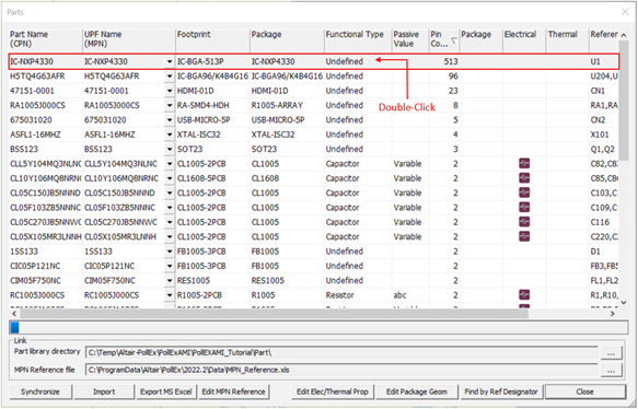
-
Double-click IC-NXP4330.
The Electrical & Thermal Properties dialog displays.
Figure 2. 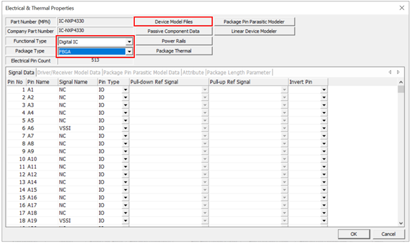
Select Digital IC as a Functional Type. Select FBGA as a Package Type. Click Device Model Files. The Device Model Files dialog displays.
- Select Digital IC as a Functional Type.
- Select FBGA as a Package Type.
-
Click Device Model Files.
The Device Model Files dialog displays.
Figure 3. 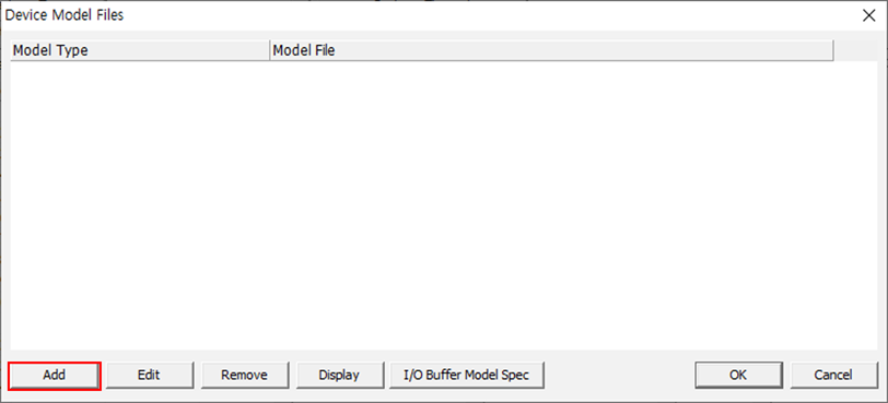
- Click Add.
-
Click
 to search and select the IBIS file
(C:\ProgramData\altair\PollEx\<version>\Examples\Solver\SI\Simulation_Model\test_ibis.ibs)
for the driver (TX) and click Open to open this file and
close this Explorer window.
to search and select the IBIS file
(C:\ProgramData\altair\PollEx\<version>\Examples\Solver\SI\Simulation_Model\test_ibis.ibs)
for the driver (TX) and click Open to open this file and
close this Explorer window.
-
Click OK to close the Model Files
dialog.
The Device Model Files dialog displays.
-
To close the Device Model Files dialog, click
OK.
When the IBIS file contains numbers of different pin count, the message like below is popped up. In this case, you click Yes.
Figure 4. 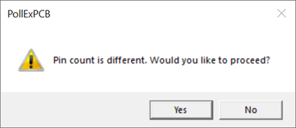
The Device Model Files dialog displays. -
Select the first line and click Display to invoke the
IBIS Manager dialog.
Figure 5. 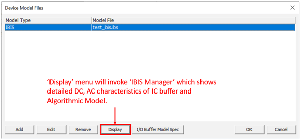
-
At the Main Information tab, you can check the
information of IBIS-AMI file like below:
Figure 6. 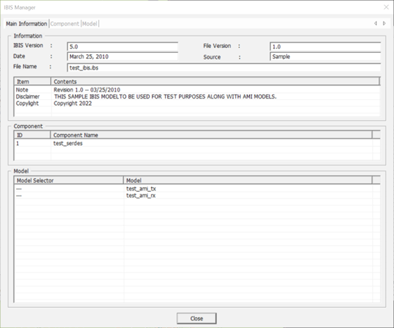
-
Click the Model tab and select Algorithmic Model.
By exploring the Algorithmic model, you can check the reserved parameters of the IBIS-AMI model about the RX and TX.
Figure 7. 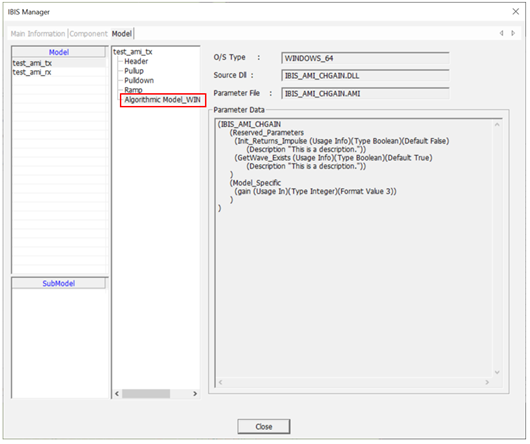
-
Click Close to disappear the IBIS
Manager dialog.
The Electrical & Thermal Properties dialog opens. The controller’s part properties are assigned automatically, as shown in the Electrical & Thermal Properties dialog.
By selecting one of the tab menus among Signal Data, Driver/Receiver Model Data, Package Pin Parasitic Model Data, and Attribute, detailed information displays.
This is the Driver/Receiver Model Data tab menu. The model file name in the red box changes depending on the IBIS model.Figure 8. 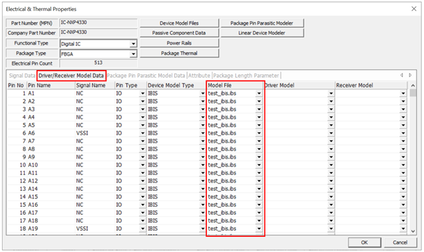
This is the Package Pin Parasitic Model Data tab menu. The parasitic values in the red box vary depending on the IBIS model.
Figure 9. 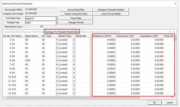
-
Click OK to close the Electrical &
Thermal Properties dialog.
The electrical icon appears.
Figure 10. 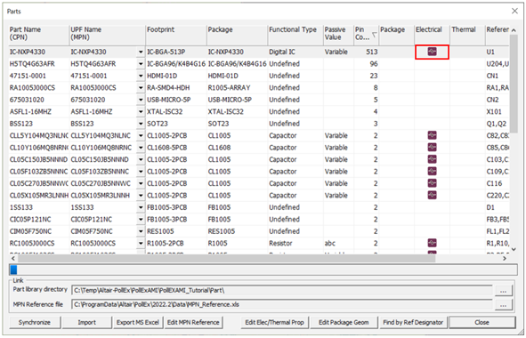
Assign SerDes Model to Connector
-
In the Parts dialog, double-click
675031020.
The Electrical & Thermal Properties dialog displays.
Figure 11. 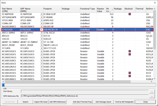
- Select Connector as a Functional Type.
- Select TO268 as a Package Type.
-
Click Device Model Files.
The Device Model Files dialog displays.
Figure 12. 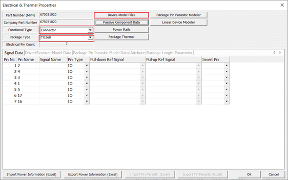
-
Click Add.
Figure 13. 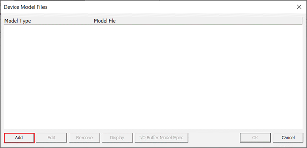
-
Click to search and select the IBIS file
(C:\ProgramData\altair\PollEx\<version>\Examples\Solver\SI\Simulation_Model\test_ibis.ibs)
for the receiver device (RX) and click Open to open this
file and close this Explorer window.
Figure 14. 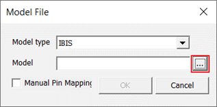
-
Click OK to close the Model Files
dialog.
The Device Model Files dialog displays.
Figure 15. 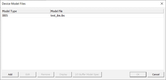
-
To close the Device Model Files dialog, click
OK.
When the IBIS file contains numbers of different pin count, the message like below is popped up. In this case, you click Yes.
Figure 16.
-
The Electrical & Thermal Properties dialog
opens.
The connector’s part properties are assigned automatically, as shown in the Electrical & Thermal Properties dialog.
By selecting one of the tab menus among Signal Data, Driver/Receiver Model Data, Package Pin Parasitic Model Data, Attribute, and Package Length Parameter, detailed information displays.
Please note that the signal name in the Signal Data tab is optional. If the user desires to write, they can fill in the Signal name. Below are some examples of Signal names for reference.Figure 17. 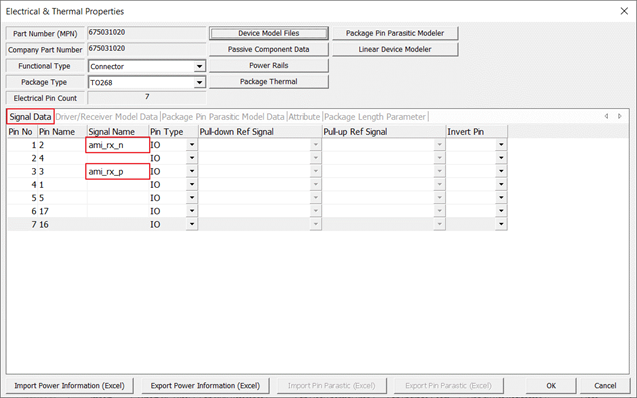
This is the tab of the Driver/Receiver Model Data.Figure 18. 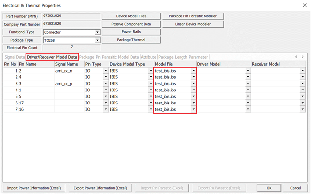
This is the tab of the Package Pin Parasitic Model Data.Figure 19. 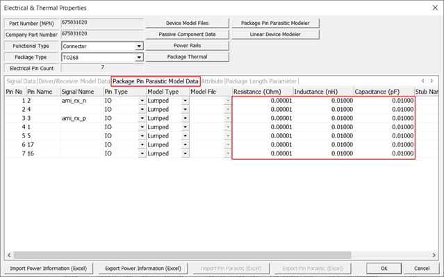
-
Click OK to close the Electrical &
Thermal Properties dialog.
The Electrical icon appears.
Figure 20. 
Define the Frequency range for SerDes Analysis
-
From the menu bar, click .
The Electrical Analysis Constraints dialog displays as below:
Figure 21. 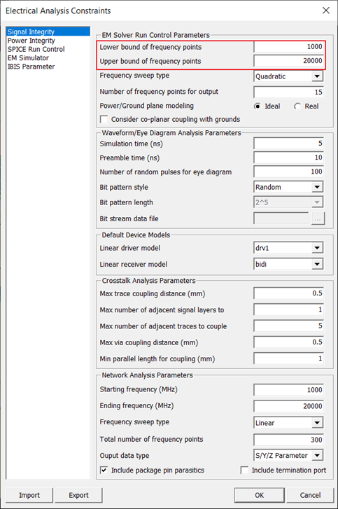
-
Change the two frequency values in the EM Solver Run Control
Parameters as follows, and these are marked with red boxes in
the above figure of the dialogue.
- Lower bound of frequency points is 1000. It means 1GHz.
- Upper bound of frequency points is 20000. It means 20GHz.
Please note that the EM Solver Run Control Parameters are frequency information used for converting PCB interconnectors into equivalent circuits for SerDes simulation.
-
Change the two frequency values in the Network Analysis
Parameters as follows, and these are marked with red boxes in
the below figure of the dialogue.
- Starting frequency (MHz) is 1000. It means 1GHz.
- Ending frequency (MHz) is 20000. It means 20GHz.
Please note that the Network Analysis Parameters refer to the following aspects:- The first aspect involves setting the frequency range for S-parameter simulation in advance. By defining this constraint, the network analysis (S-parameter) will automatically use the specified frequency range during simulation.
- The second aspect pertains to the frequency range used for calculating the impulse response required for SerDes simulation. This tool utilizes an algorithm that converts S-parameters into impulse responses to compute the impulse response of the object within the defined frequency range.
Figure 22. 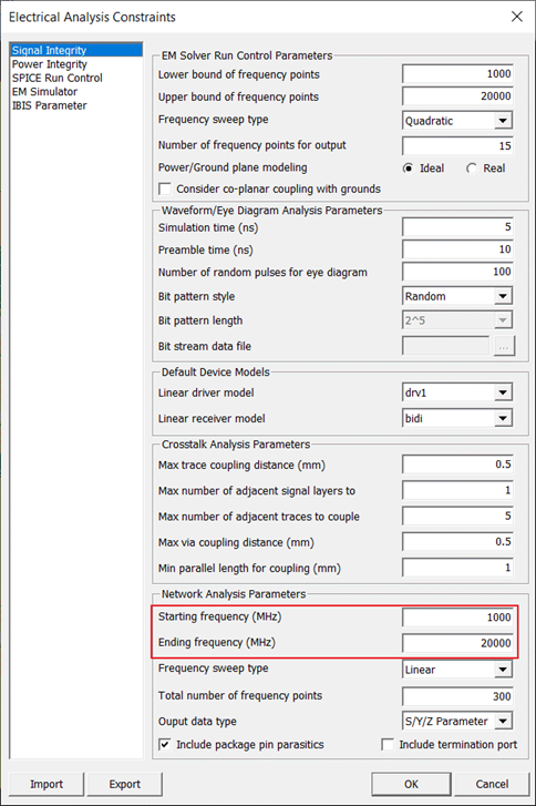
Network Analysis (Waveform)
- Click > > .
-
Click Select Net and select
MCU_HOST_USB+ and click
OK.
Figure 23. 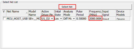
Figure 24. 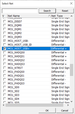
- You can set Frequency for the signal on Network analysis dialog and then choosing the U1-D25 as the Active Driver Pin.
- Click Device in the Network Analysis dialog.
-
Check the connected components and pins to the selected net using the
Device Model List dialog and click
OK.
Figure 25. 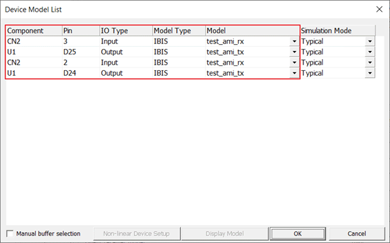
-
Changing the Simulation times (ns) to 2 and Signaling time (ns) to 2 and then
click Analyze.
When the waveform analysis starts, electromagnetic simulation extracts the SPICE model for the selected net.
The excitation source signal is applied to the net which is specified by the assigned pin model’s operating characteristics and the values defined at Input Signal and Pulse Period. When the simulation is done, the Waveform Viewer opens or exploring the waveforms.Figure 26. 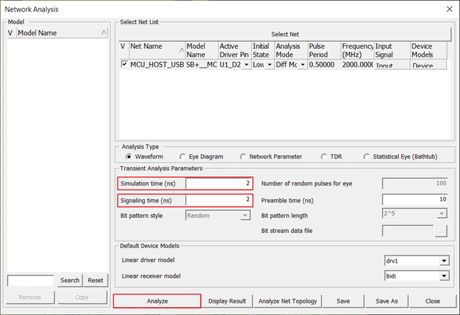
-
After the simulation, Waveform Viewer dialog opens.
Result A: All waveform for TX and RX is displayed.
Figure 27. 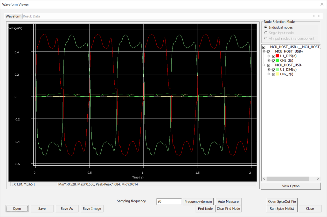
-
Uncheck the CN2_2(i) and
CN2_D3(i) to check for RX waveform. Right click and
select Zoom all button.
Result B: Waveform for RX is displayed.
Figure 28. 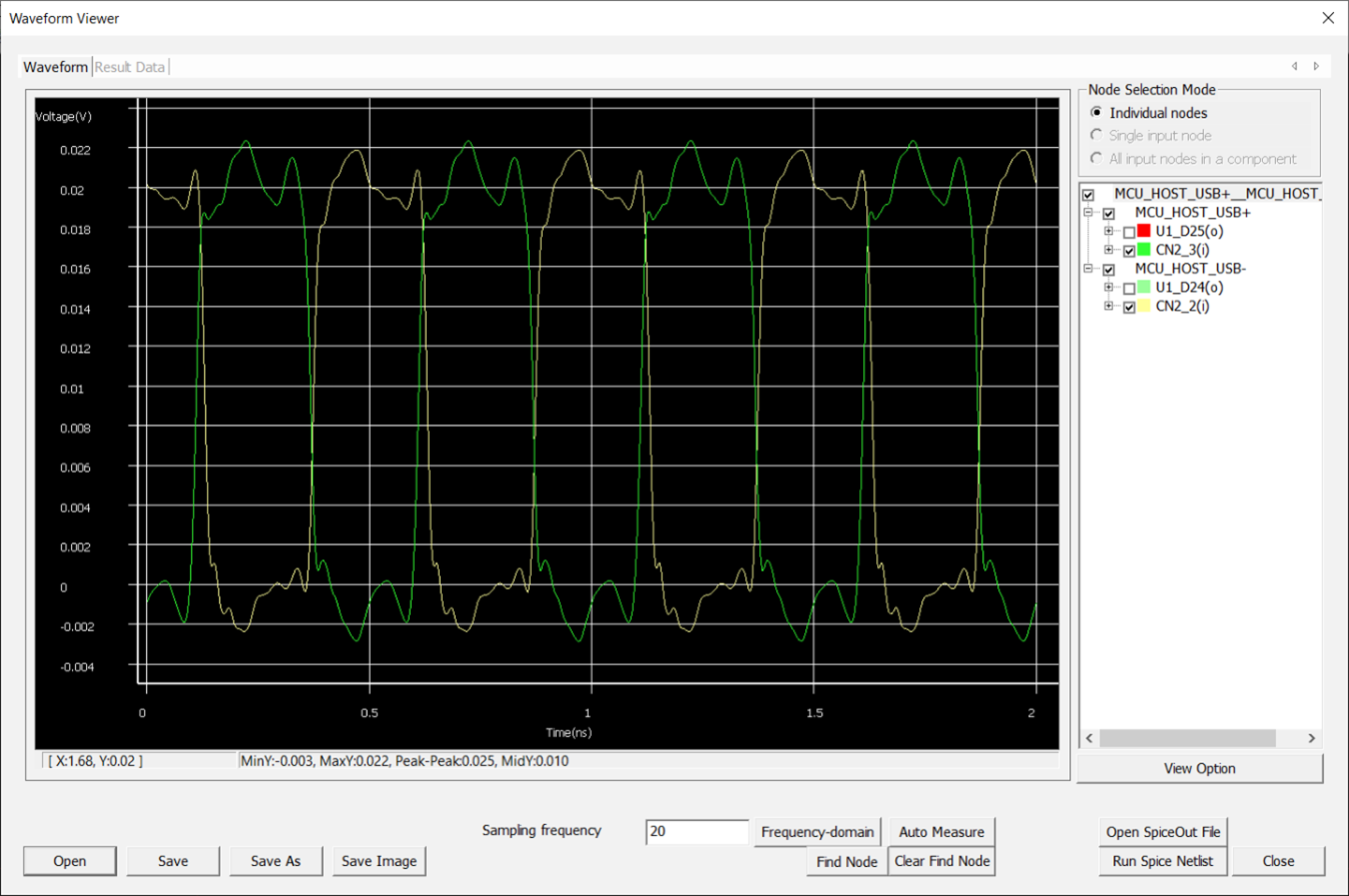
- For checking the impulse response, uncheck all waveform and select IO_CN2_3.IMPULSE. And then right click and select zoom all.
-
Uncheck all waveform, right click IO_CN2_3.IMPULSE and
select zoom all to verify the impulse response.
Result C: Waveform for Impulse response is displayed.
Figure 29. 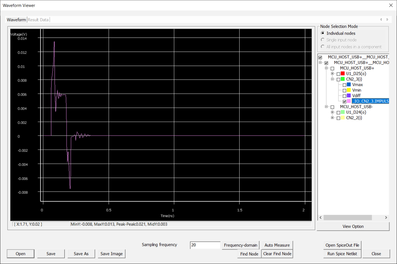
Network Analysis (Eye-diagram)
- Select Eye Diagram for Analysis Type.
-
Select the net, MUC_HOST_USB+.
Figure 30. 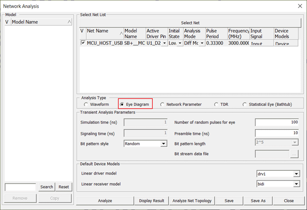
-
Click Analyze.
After the simulation, Waveform Viewer dialog displays.
Figure 31. 
This is an eye diagram representing 100 bits accumulated in a period. It shows the automatically selected Rx-side differential lines, CN2_2(i) and CN_3(i).
- Close the Waveform Viewer dialog.
Network Analysis (Statistical Eye)
- Select Statistical Eye (Bathtub) for Analysis Type.
-
Select the net, MUC_HOST_USB+.
Figure 32. 
-
Change the Baud Rate (Gbps) to 4 and NoiseRMS to 0.003 and then click
Analyze.
After the simulation, Statistical Eye Analysis Result dialog opens.
Figure 33. 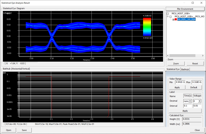
- Click Close.
- Push again the Display Result button in the Network Analysis dialog.
-
By pressing the Measure button and checking
Line X and Distance X, user
can manually measure the eye width at the desired position as below:
The value is 0.2727 (ns) in this case. Please note that the measured distance value is changeable depending on which point the user clicks.
Figure 34. 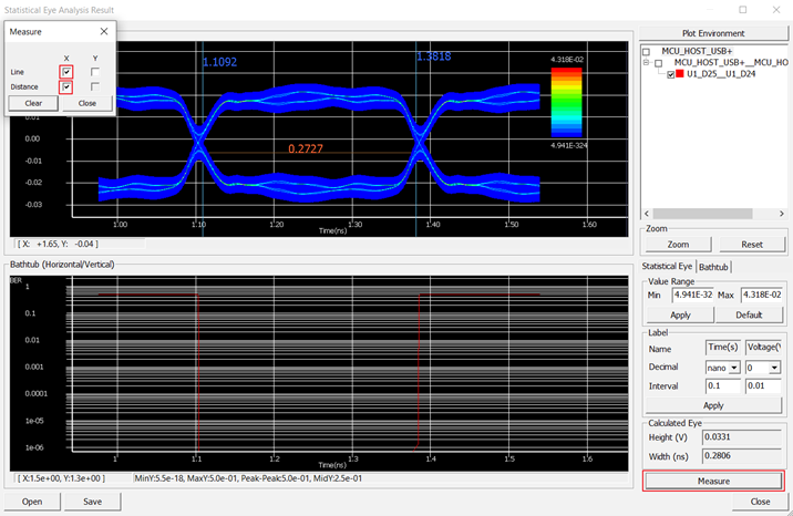
Network Analysis (Bathtub Curve)
- Select Statistical Eye (Bathtub) for Analysis Type.
-
Select the net, MUC_HOST_USB+.
Figure 35. 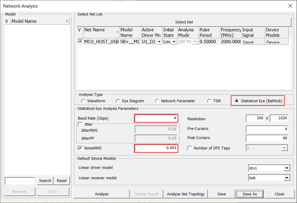
-
Click Analyze after changing the Baud Rate (Gbps) to 4
and NoiseRMS to 0.003.
Please note that if the Statistical Eye simulation has already been completed in the previous case, there is no need to perform the analysis again. So just push again the Display Result button in this dialog.After this, Statistical Eye Analysis Result dialog opens.
-
Clicking on the Bathtub tab located on the right side of
the dialog allows the user to set up the Bathtub curve plot.
Figure 36. 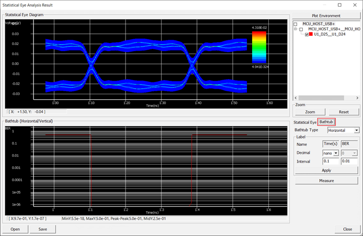
- Click on the Measure button, keeping the selection of the Bathtub type to be Horizontal.
-
Fill in the BER value as 1e-5 and click on the Add
button. This will plot the Timing margin (ns) value at the BER of 1e-5 as
below.
The result value is 0.2797 (ns) in this case and it also shows the distance mark at the bathtub curve in the Statistical Eye Analysis Result dialogue.
Figure 37. 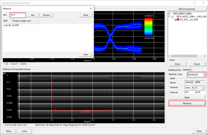
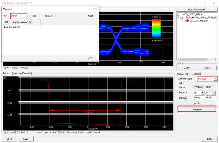
- Change the Bathtub type to Vertical and click on the Measure button.
-
Fill in the BER value as 1e-13 and click on the Add
button. This will plot the Voltage margin (V) value at the BER of 1e-13 as
below.
The result value is 0.0372 (V) in this case and it also shows the distance mark at the bathtub curve in the Statistical Eye Analysis Result dialogue.
Figure 38.