PollEx PCB is a design browser (viewer) from various ECAD
vendors.
PollEx PCB supports CADENCE,
Mentor Graphics, Zuken, Altium, and different standard neutral files. To open the PCB press F1 or click Help > PollEx Manual from the menu bar.
Open and Save PollEx PCB Layout Design File
From the Home ribbon of the PollEx Launcher, click
PollExPCB.
Figure 1.
From the menu bar, click File > Open and open the
PollEx_PCB_Sample_r<revision_number>.pdbb
file from
C:\ProgramData\altair\PollEx\<version>\Examples.
From the View tab of the menu bar, adjust the display
controls.
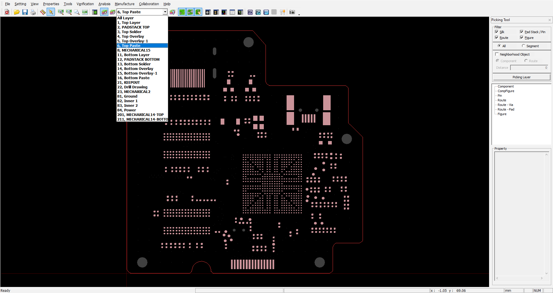
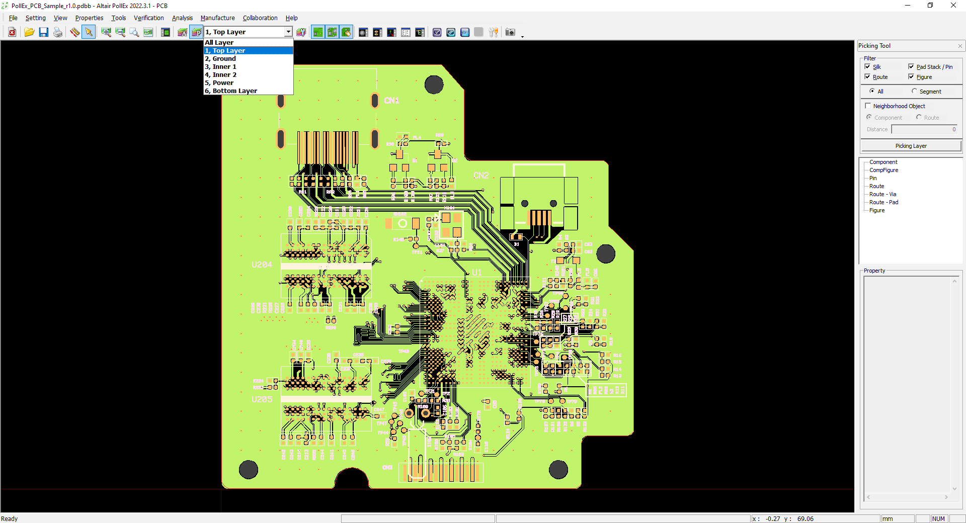
Change the layer display.
From the toolbar, click and select 6, Top
Paste.
Figure 2.
Shape data on Top Paste displays. You can display and see the layer by
selecting the name on the list.
From the toolbar, click and select 1, Top
Layer.
Figure 3.
Combined layers as Top Layer is shown on the window.
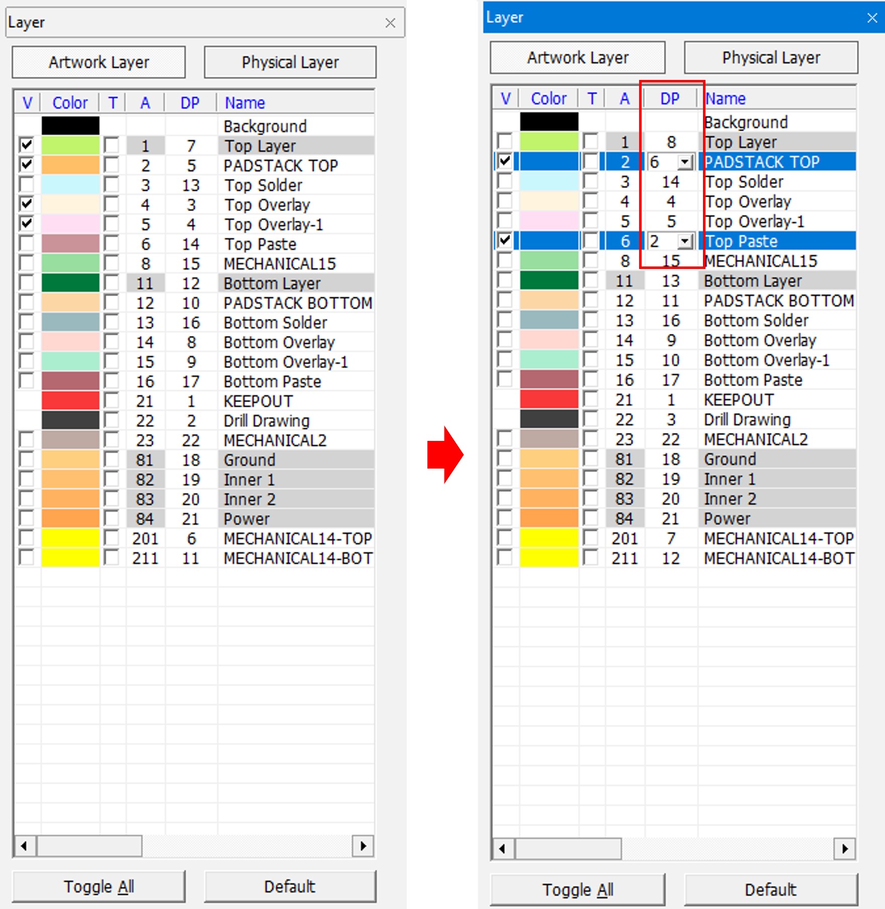
Display the target layer(s).
From the menu bar, select Setting > Layer.
In the Layer dialog, select PADSTACK
TOP and Top Paste.
For Top Paste, change the DP value to 2.
Figure 4.
Top Paste is overlapped on the PADSTACK TOP layer.
Close the Layer dialog.
Setup Property of PCB Objects
In this step, you will setup the property of PCB objects, nets, components, and
others.
The Picking tool is used to check the object information and property included in the
PCB design data. When the PollEx PCB program is initiated,
the Picking tool is automatically enabled on the right-side of the application.
From the menu bar, click Setting > Picking to disable the Picking tool.
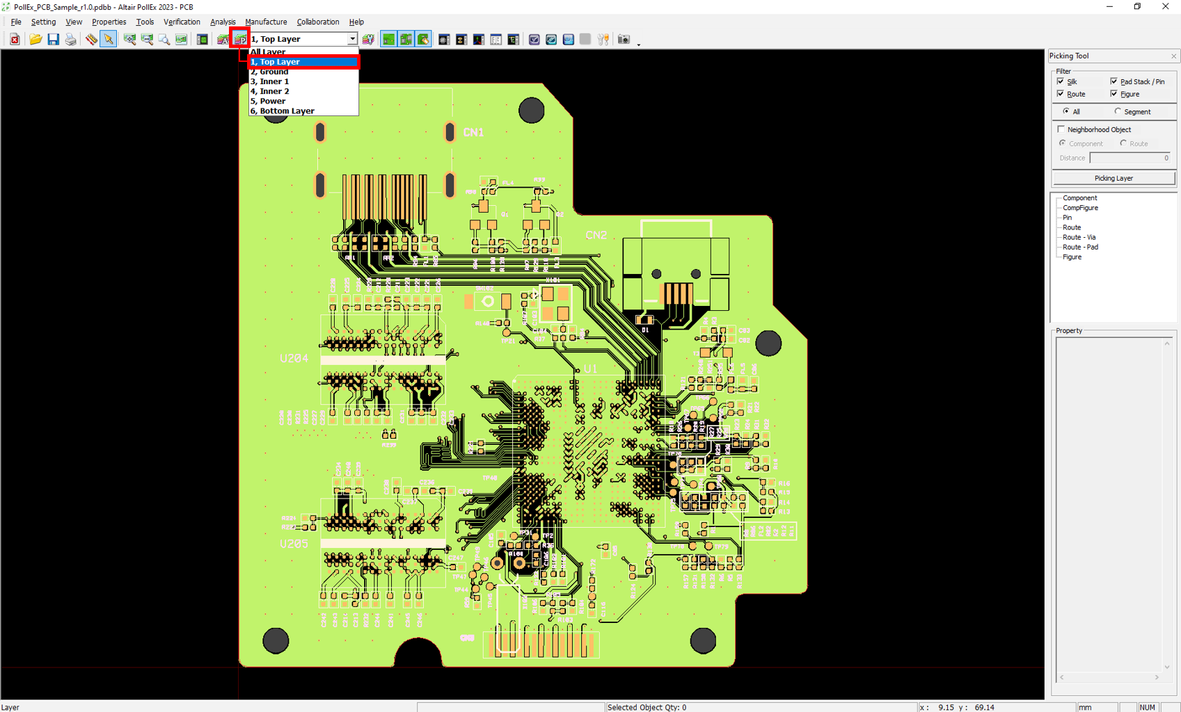
Find object properties using the Picking Tool.
From the toolbar, click and select 1, Top
Layer.
Figure 5.
In the window, select an object within the design.
The object name and property information display.Figure 6.
Find objects in the PCB design using the PCB Explorer.
The PCB Explorer finds parts and nets in the design data.
From the menu bar, click Tools > PCB Explorer.
From the PCB Explorer, use Selection Type A and B to check the
connected part, reference, and net name.
From the Selection Type A section, select Part, Reference, or Net and
enter a name in the search field.
Use the Picking tool and PCB Explorer to review the connected information of
parts or nets.
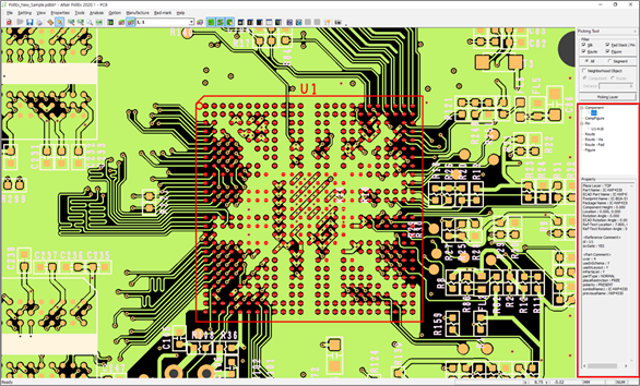
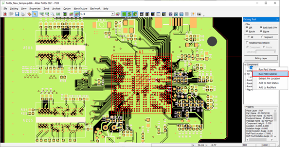
In the window, select a component.
In the Picking tool window, right-click the component name and select
Run PCB Explorer from the menu bar.
Figure 7. In this tutorial, U1 is selected.
In the PCB Explorer, Selection Type – B, select
Net and click
Disp.
The selected nets with the connected component
display.
Close the PCB Explorer.
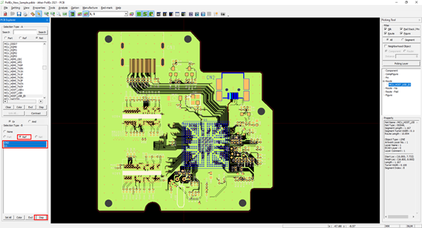
Check the component connected to the net.
In the window, select a Net to check.
From the Picking tool, right-click the Route name and select
Run PCB Explorer from the context menu.
Figure 8. Figure 9.
From the PCB Explorer, Selection Type – B section, select
Ref.
From the Selection Type – B section, select the names and complete one
of the following options:
Click Disp to display the selected nets
with connected components.
Click Excl to display only the selected
objects, other objects are not displayed.
Close the PCB Explorer window.
Measure the distance between objects.
From the menu bar, click Setting > Measure to launch the Measure tool.
The Measure tool opens on the right-side of the
window.
From the Measure tool, select Point to Point to measure between
locations.
In the application, click two points.
From the Measure tool, select Component to Component to measure between
components.
In the window, select two points.
From the Measure tool, Option section, select Keep to maintain the
measured results.
From the toolbar, click to close the Measure tool and open the
Picking tool.
Click to reset the view in the window.
Various Object Viewers
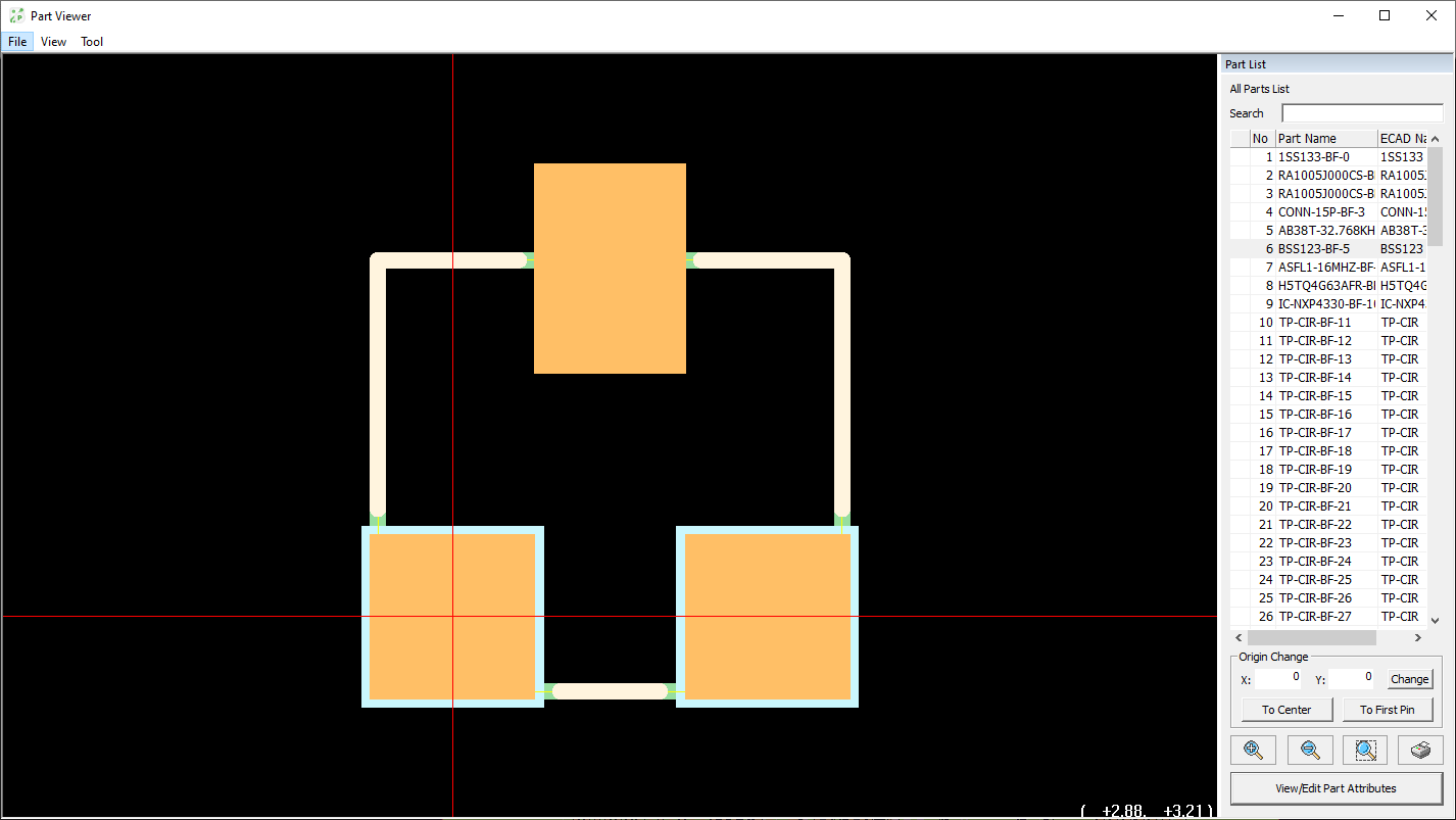
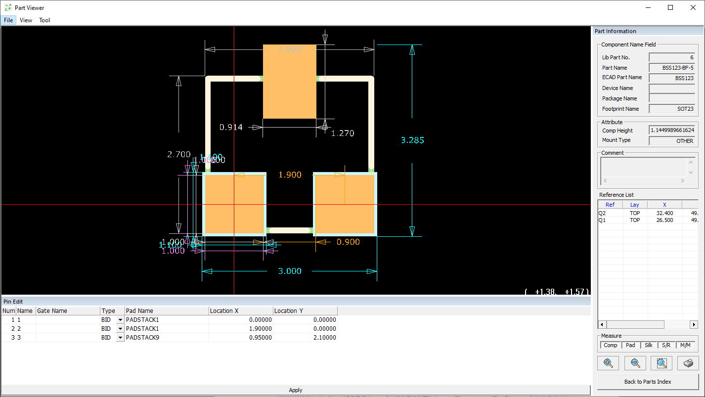
From the menu bar, click Tools > Part Viewer.
The Part Viewer dialog opens.
From the Part Viewer dialog, select a part from the part
list or use the search bar to find the desired part.
Figure 10. The selected part shape is displayed in the dialog. The red axis is the
origin point of the part, from the part library.
Once a part is selected, click View/Edit Part
Attributes.
Figure 11.
Check the pin information of the selected part by completing one of the
following options.
Check the reference name list with the same part name, Layer location,
and Layer coordinates.
Check the dimension information using the Comp, Pad, Silk, S/R, M/M
buttons.
Check the Pin name and location of the selected part.
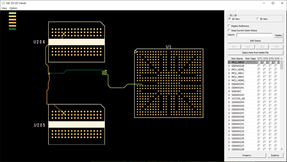
From the menu bar, click Tools > Net 2D/3D Viewer.
Use the Net 2D/3D Viewer to check nets connectivity and their
three-dimensional structures. Run the Net 2D/3D viewer to see a 2D image with
net lists and connected components, as shown in the following image.Figure 12. Use the search field to search by net name or select from the netlists. If
a net is selected, the selected net displays in the dialog. To check the net in
3D, select 3D View from the 2D/3D section.
Check the net structure and properties.
Select 3D View from the 2D/3D section.
From the net list, select MCU_ABA0.
Rotate the selected net by completing one of the following
options:
Use the arrow buttons in the Net 3D Viewer Rotation menu.
Move your mouse while holding left-mouse click.
Click Property.
Click each item under MCU-ABA0 to see each structure in the net routing
pattern.
Close the Net 2D/3D Viewer dialog.
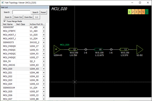
From the menu bar, click Tools > Net Topology Viewer.
The Net Topology Viewer dialog opens.
Use the Net Topology Viewer to
check a net with a topology structure (Driver-Load-Receiver) including
connected Vias and Branches. The viewer configures the net length and width
of a trace and a component by displaying different colors per
layer.
From the Net List, select MCU_D20.
Figure 13. MCU_D20 displays as the topology structure with the following parameters:
: placed layer and color
Driver
W: net width
L: net length
Change the Active Port Name to U1_D2.
Figure 14.
Close the Net Topology Viewer dialog.
Make Comments on PCB
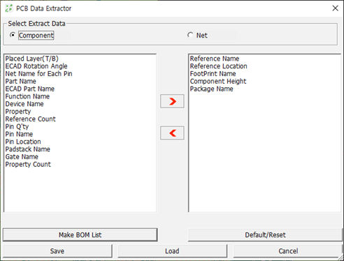
The PCB Data Extractor generates a document of component and net information that can
be exported as an Excel file.
Use the PCB Data Extractor to export component and net information.
From the menu bar, click Tools > PCB Data Extractor.
The PCB Data Extractor dialog
opens.
Use the red arrows to move items to be documented from the left column
to the right.
Figure 15.
After the necessary items are selected, click Make BOM
List.
The PCB Data Extractor Result dialog
opens.
To export an Excel file, click Export to
MS/Excel.
To export Net information (Net length, connected via, total via
numbers, and so on), select Net in the
PCB Data Extractor dialog and repeat steps
1.b –
1.d.
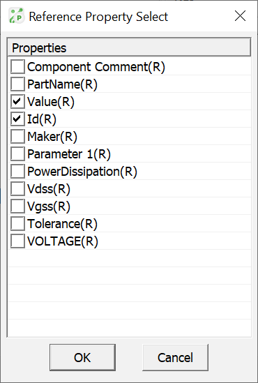
Export a report with reference property.
From the PCB Data Extractor dialog, move
Property from the left column to the right
using the red arrows.
The Reference Property Select dialog
opens.
Enable the checkboxes of the necessary properties to be included in the
document and click OK.
Figure 16.
The selected properties display in the right
column.
To save the environment for making a report, click Save
or Load in the PCB Data Extractor
dialog.
The environment is saved as an *.pdt
file.
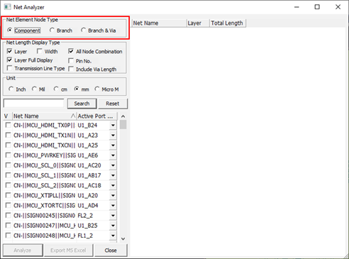
Use the Net Analyzer tool.
The Net Analyzer is used to analyze all net length information by considering
Layer, Branch, and Via location.
From the menu bar, click Tools > Net Analyzer.
The Net Analyzer dialog opens.
From the Net Analyzer dialog, verify the Net
Element Node Type is set to Component.
Figure 17. Net Element Node Type options:
Component: net length among components.
Branch: net length among components, including length of
branched points.
Branch & Via: net length among components, branching points,
and vias.
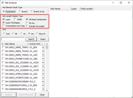
Select at least one item to be displayed.
Figure 18. Net Length Display Type options:
Layer: display net length by a layer.
Width: display routing pattern width.
All Node Combination: display all combination of nodes.
Layer Full Display: display stack-up information and net length
by a layer.
Pin No: display component pin number.
Transmission Line Type: display lengths of micro strip line and
strip line.
Include Via Length: display via information.
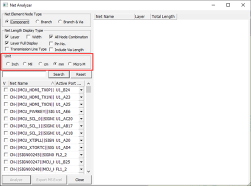
Select a display unit.
Figure 19.
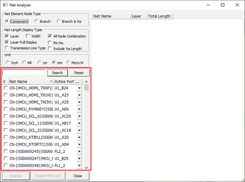
Use the search bar to find the desired net name.
Figure 20.
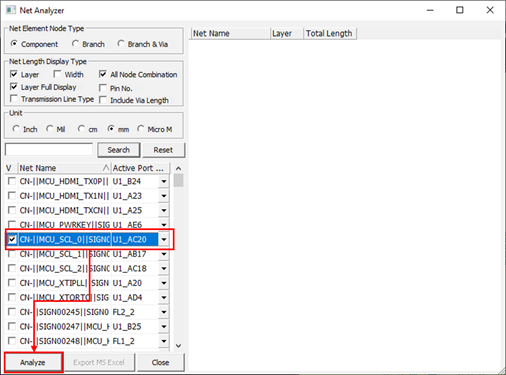
Enable the checkbox of the desired Net and click
Analyze.
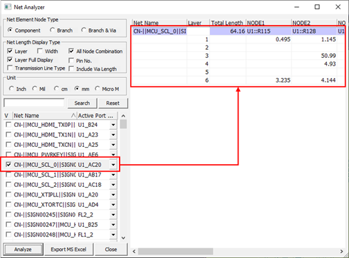
Figure 21. The length information of the selected net displays.Figure 22.
To make a report, click Export MS Excel.
Close the Net Analyzer Report dialog and click
from the toolbar.
Execute Redmark.
From the menu bar, click Collaboration > Redmark.
The Redmark dialog opens on the left side
of the application.
From the Redmark dialog, click
Add.
Enter a title and any other necessary information.
In the Add Draw Object area, define the width, start type, and end
type.
Select the object shape and draw the object in the window.
Click Done.
The comment displays in the list.
Save Redmark file (*.prmk).
You can save in *.prmk or *.pdbb
format. Saved files can be shared with others to check the comments.
Complete one of the following options:
To save in *.prmk format, click
Save from the
Redmark dialog.
To save in *.pdbb format, from the menu bar, click File > Save As.
Select a file location, input the file name, and click
Save.
Load a Redmark file.
Complete one of the following options:
To open a *.prmk file, click
Load from the
Redmark dialog.
To open a *.pdbb file, from the menu bar, click File > Open.
Useful Functions for Engineers
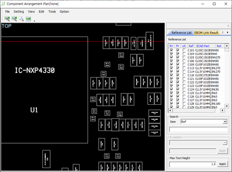
Use the Component Arrangement Plan tool to create a work-plan sheet. Using the
created format, you can also apply this format to other designs to make another work-plan
sheet.
From the menu bar, click Tools > Component Arrangement Plan.
Click Setting > CAP Data Setting.
The Component Arrangement Plan Setting
dialog opens.
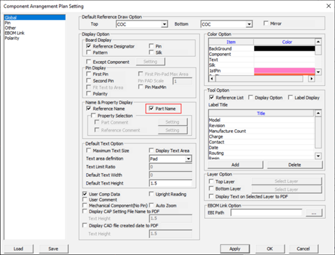
In the Component Arrangement Plan Setting dialog,
enable the Part Name checkbox and click
OK.
Figure 23. The part name displays in the Component Arrangement
Plan dialog.Figure 24.
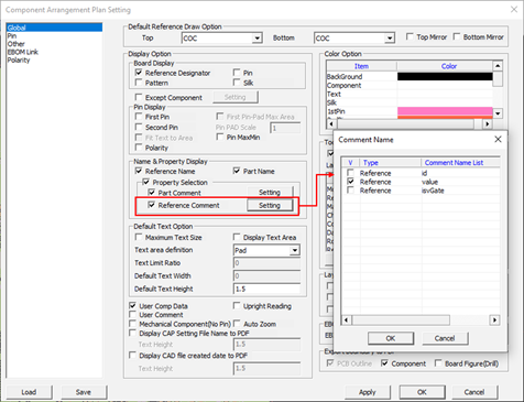
From the Component Arrangement Plan dialog
menu bar, click Setting > CAP Data Setting.
The Component Arrangement Plan Setting
dialog opens.
From the Component Arrangement Plan Setting
dialog, enable the Property Selection
checkbox.
From the Comment Name dialog, select the value and
click OK.
If there is no value in the part property, you can select value
in Reference Comment as shown below.Figure 25. Figure 26.
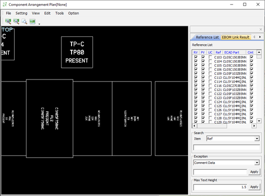
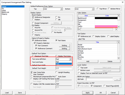
From the Component Arrangement Plan Setting
dialog, select COC for Text Area Definition and click
OK.
Figure 27. The text for reference name and value is displayed in the COC
area.
Display first pin location.
From the Component Arrangement Plan dialog
menu bar, click Setting > CAP data setting.
The Component Arrangement Plan Setting
dialog opens.
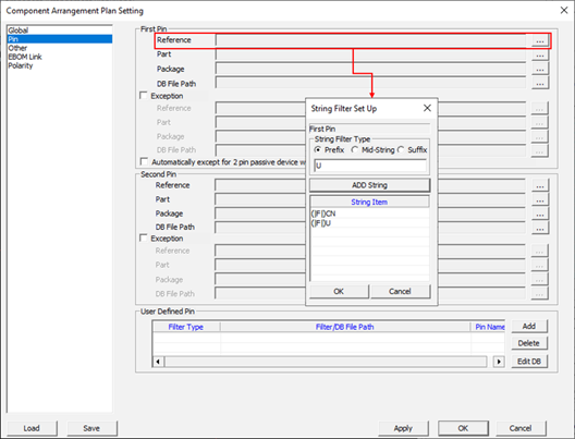
Select Pin.
At the end of the Reference field, click the ellipses.
The String Filter Set Up dialog
opens.
From the String Filter Set Up dialog, enter
U and CN for reference
prefix recognition.
Figure 28. References with names starting with U and CN are shown with their
1st pin location.
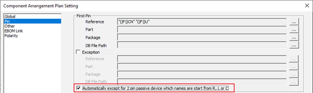
In the Component Arrangement Plan Setting dialog,
enable the Automatically except for 2 pin passive device
which names are start from R, L or C checkbox and click
Global.
Two pin components that have a reference name starting with ‘R, L, C’
will not display in the 1st pin’s location.Figure 29.
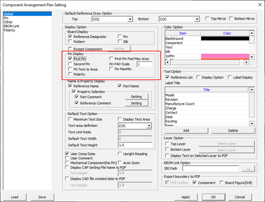
From the Pin Display section, enable the First
Pin checkbox and click OK.
Figure 30. References with names starting with U and CN are shown with their
1st pin location.
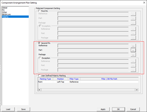
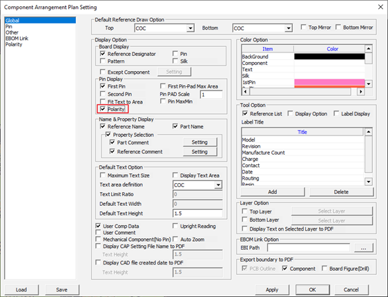
Display component polarity.
For components with polarity like a capacitor, you can display their
polarity.
From the Component Arrangement Plan dialog
menu bar, click Setting > CAP Data Setting.
The Component Arrangement Plan Setting
dialog opens.
In the Component Arrangement Plan Setting dialog,
select Polarity.
Enable the Second Pin checkbox.
Figure 31.
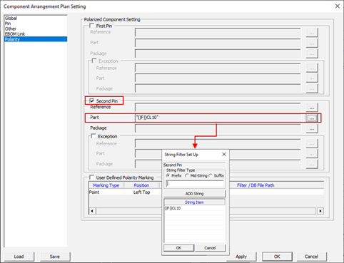
Click the ellipses at the end of the Part field.
The String Filter Set Up dialog
opens.
In the String Filter Set Up dialog, enter
CL10, press Enter, and
click OK.
Figure 32. This displays the polarity on the second pin of the part whose
part name starts with CL10.
Select Global, enable the Polarity checkbox from
the Pin Display section, and click OK.
Figure 33.
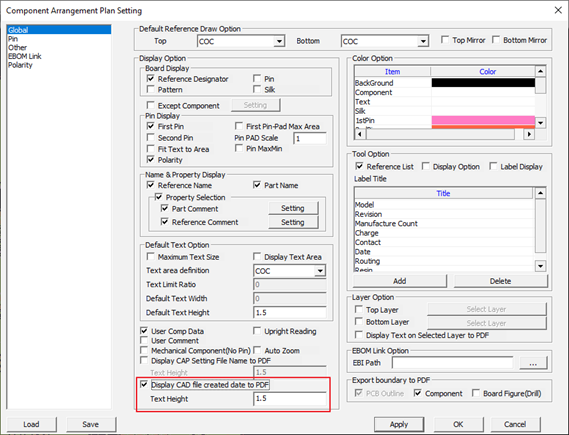
Output completed work-sheet.
From the Component Arrangement Plan dialog
menu bar, click Setting > CAP Data Setting.
The Component Arrangement Plan Setting
dialog opens.
In the Component Arrangement Plan Setting dialog,
enable the Display CAD file created date to PDF
checkbox and click OK.
This option shows the design creation date.Figure 34.
From the Component Arrangement Plan dialog
menu bar, click File > Print.
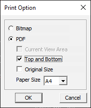
The Print Option dialog opens.
From the Print Option dialog, select
PDF and enable the Top and
Bottom checkbox.
Verify the Paper Size is set to A4 and click
OK.
Figure 35.
Specify a save location, enter a file name, and click
Save.
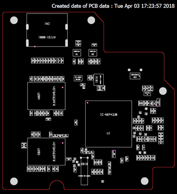
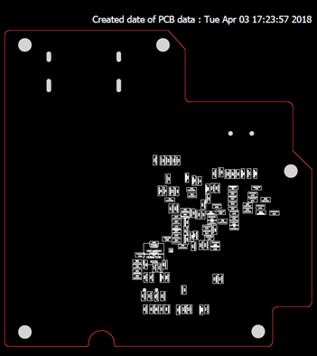
A worksheet for the top and bottom is output into a PDF file Top
side worksheet. Bottom side worksheet.
Top side worksheet.Figure 36. Bottom side worksheet.Figure 37.
Set file for worksheet saving and loading.
From the Component Arrangement Plan dialog
menu bar, click File > Save.
Specify a save location, enter a file name, and click
Save.
The file extension is *.capb. The setting files
saved contents can be used for the same design or other designs.
Load a saved setting file.
From the Component Arrangement Plan dialog
menu bar, click File > Load.
Browse to the desired file and click Open.
Close the Component Arrangement Plan dialog.
Restricted PDBB
Use PollEx PCB to change its design. Partially remove or
hide some objects in the design.
If you want to share the PCB layout design with restricted objects or information
such as certain components and nets, use Restricted PDBB to save as edited PDBB.
Run Restricted PDBB.
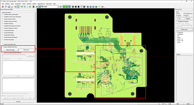
From the menu bar, click File > Export To > Restricted PDBB.
The Export Restricted PDBB menu shows on the left side of
application.
From the Export Restricted PDBB menu, enable the Remove
Board-Contour and Include Metal
Mask check boxes.
Click Save As.
Specify a save location, enter a file name, and click
Save.
The Exported Restricted PDBB file is saved with the selected
conditions.
From the Export Restricted PDBB menu, select Export Selected
Area Only and click Select
Area.
In the window, draw an area to save and press
Enter.
Figure 38.
From the Export Restricted PDBB menu, click Save
As.
PollEx Real PCB Assembly View Tutorial
Use the Real PCB Assembly Viewer to transform a design into 3D shapes and export data
into STEP format to link to a mechanical CAD system.
From the PollEx Launcher, Home ribbon, click the
PollExPCB.
From the menu bar, click File > Open and open the file,
C:\ProgramData\altair\PollEx\<version>\Examples\PollEx_PCB_Sample_r<revision_number>.pdbb.
Note: Refer to the PollEx PCB manual about how to use the
PollEx PCB viewer.
Save as Project.
PollEx PCB operates on a design project database
which contains the data of a PCB design including the materials, parts, physical
layout, analysis models, and analysis result data. With the unified design
project database, this application can be commonly used by multiple engineering
disciplines.
From the menu bar, click File > Save As Project.
The Save As Project dialog opens. The
sample PCB design name displays as the New project name.
From the Save As Project dialog, click
OK.
Link components.
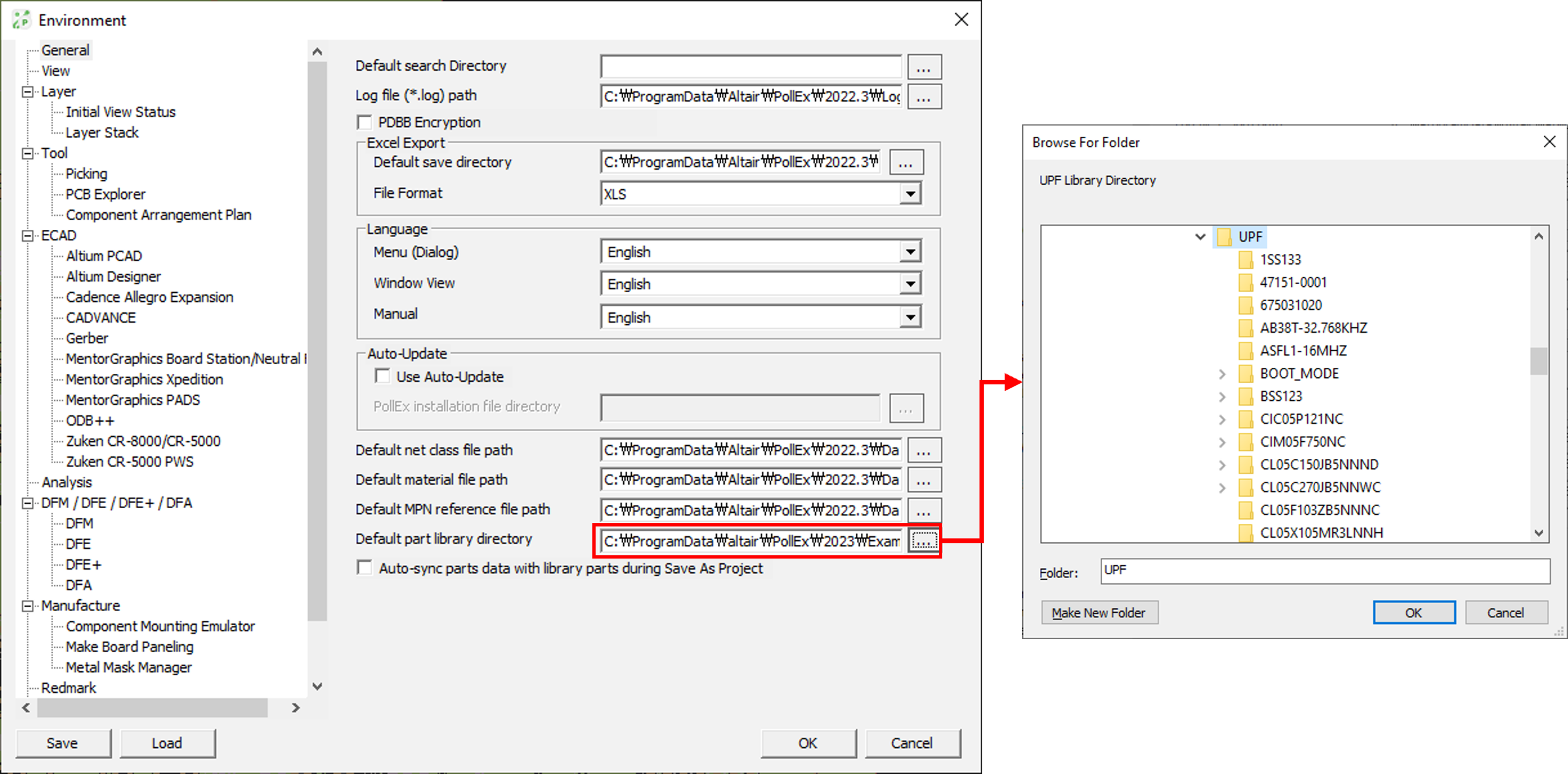
From the menu bar, click Setting > Environment.
The Environment dialog opens. You can set
the environment for importing 3D part libraries.
From the Environment dialog, click the ellipses at
the end of the Default part library directory field to define the
default 3D part librarian path.
Define the unified part library directory found here:
ProgramData\altair\PollEx\<version>\Examples\UPF.
Figure 39.
Click OK.
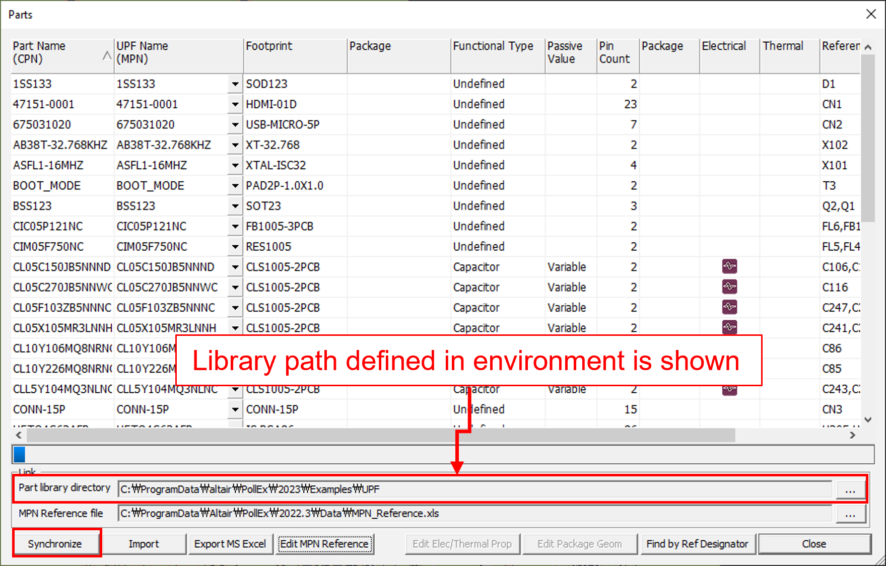
From the menu bar, click Properties > Parts.
The Parts dialog opens.
From the Parts dialog, click
Synchronize.
Figure 40.
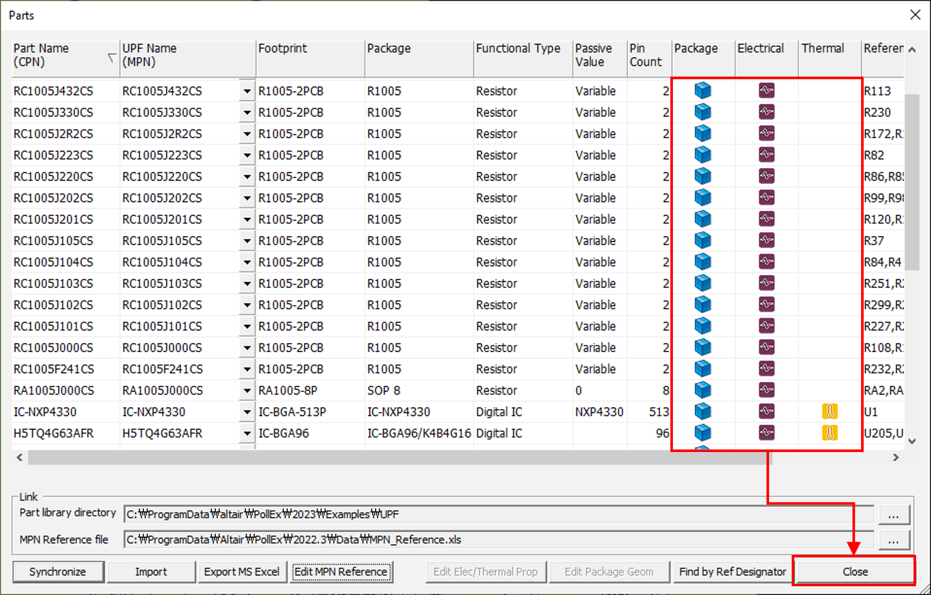
The image below shows the parts linked status.Figure 41.
: Linked to 3D packages
: Linked to electrical buffer
model
: Linked to package thermal
libraries
Click Close.
Run Real PCB Assembly Viewer.
From the menu bar, click Tools > Real PCB Assembly Viewer.
The Real PCB Assembly Viewer dialog
opens.
To review the design, hold left mouse click and rotate your
cursor.
From the Real PCB Assembly Viewer dialog menu bar, click View > Route.
Review the design routing status.
From the Real PCB Assembly Viewer dialog menu bar, click Tools > Board
X/Y Cut.
The Board X/Y Cut dialog
opens.
Use the Board X/Y Cut dialog to review the cutting
edge of the design along the X or Y axis and click
Close.
Measure between components.
Click Tools > Measure.
The Measure dialog opens.
Use the Measure dialog to measure between
components.
Close the Measure dialog.
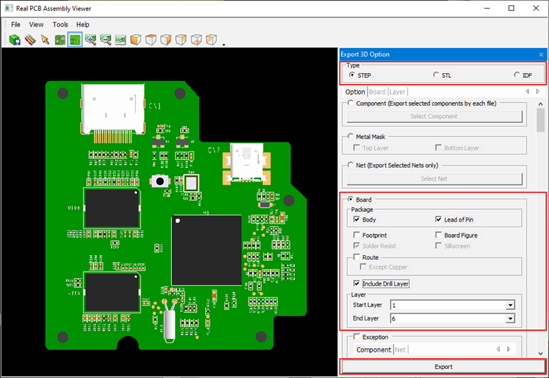
Export to 3D Format. Designs can be exported in the following formats: STEP,
STL or IDF.
In the Real PCB Assembly Viewer dialog, click File > Export To > 3D Format.
The Export 3D Option dialog
opens.
From the Export 3D Option dialog, select an export
type, define the board settings, and click
Export.
Figure 42.
Specify a location, enter a file name, and click
Save.
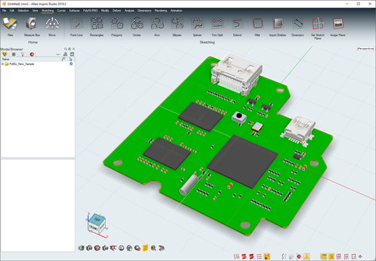
Use a mechanical CAD or MCAD system to read the exported STEP
file.Figure 43.
 and select 6, Top
Paste.
and select 6, Top
Paste.
 and select 1, Top
Layer.
and select 1, Top
Layer.
 to close the Measure tool and open the
Picking tool.
to close the Measure tool and open the
Picking tool.
 to reset the view in the window.
 : placed layer and color
 : Linked to 3D packages
 : Linked to electrical buffer
model
: Linked to electrical buffer
model : Linked to package thermal
libraries
: Linked to package thermal
libraries