Differential Pair Nets
Differential pair nets are routing patterns with a certain parallel clearance apart on which reversed signals flow at the same time to send information.
- Item: Input item name.
- Net: Select Differential Pair Net Group.
- Filter: Enter a filter to choose differential pair net from selected net group. After entering a base net and pair net add them into the list by clicking Add Filter.
- Coupling Ratio (%): Ratio (%) of parallel length that satisfies the
differential pair separation condition with total net length. Lower ratio
will be a fail in the report.
- Ratio Fail: If result ratio is lower than this value, violating regions are displayed in yellow and acceptable regions are displayed in cyan.
- Separation Tolerance (%): Tolerance (%) to measure an allowable distance between nets in a differential pair.
- Separation: Define parallel segment separation criteria. If you do not enter any specific value, the DFE uses the longest net’s separation by default.
- Each Layer: Define different separation values for different layers.
- Layer No: Define layer number. If you do not enter any specific value, the DFE gets layer number from PCB property by default.
- Separation (Each Layer): Define different separation values for different
layers.
- Separation: Required separation for each layer.
- Use the separation of longest segment pairs: The DFE uses the longest net’s separation by default. (per layer)
- Pin Escape: Enter a radius of circular region around pins to be excluded for the rule check.
- Component Keep IN/OUT: Define test region. For example, you can test inside
or outside the breakout region of CPU with different test
values.
- Component Group: Select required component group which is used for defining the test region.
- Region: Define the required test region.
- IN: DFE tests the inside of the breakout region of target component.
- OUT: DFE tests the outside of the breakout region of target component.
- Range (COC+distance): Enter the distance value to define breakout range. The COC (Component Overlap Check) plus this distance value is considered the test range.
- Target Layer: Select the required test layer.
- All Layer: Test all layers.
- Component Place Layer: Test only component placement layer.
- Different Rule Setup in Special Region: Assign additional test
region for breakout region testing.
- Extended Region from COC: Enter the distance value to define additional range. The COC (Component Overlap Check) plus this distance value is considered the additional test range.
- Allowable Values: Assign additional allowable test value for this additional region.
- Value: Add additional allowable value.
- Range: Add additional allowable range.
- Deviation: Add additional allowable value with deviation using this option.
- Deviation (%): Add additional allowable value with deviation (%).
- The test range and test values will be:
- Case1: Component Keep In region test
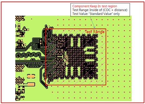
Figure 1. - Case2: Component Keep Out region test
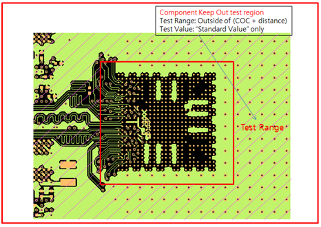
Figure 2. - Case3: Component Keep Out with extended region test
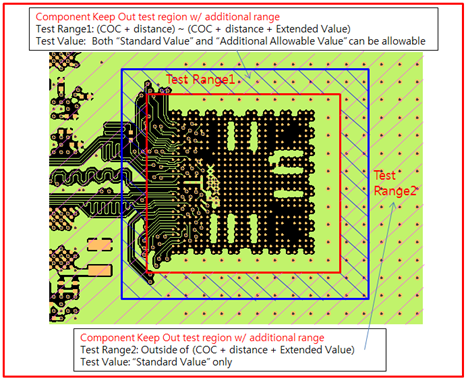
Figure 3.
- Case1: Component Keep In region test
- Composite Net Separation Check: Checks if there is composite net.
- Composite Component: Select the composite component.
- TP Separation Check
- TP Component: Specify used test-point component group.
- TP Separation: If test-points are used as pair, specify the distance between test-components.
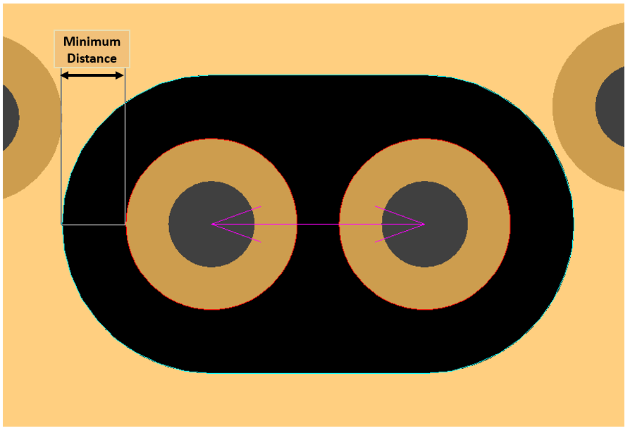
- Nut Shape Anti-Pad: Checks whether the shape of anti-pad form a closed nut
shape.
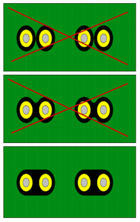
Figure 4.- Except Layer: Select exception layers to exclude Nut Shape Check.
- Minimum distance : Set minimum distance between via and
anti-pad.
- Passive Component Fill-cut check: Checks if there is passive component
fill-check on pcb design.
In PCB design, "fill" and "cut" refer to the placement of copper planes or traces in relation to the routing of a differential signal line.
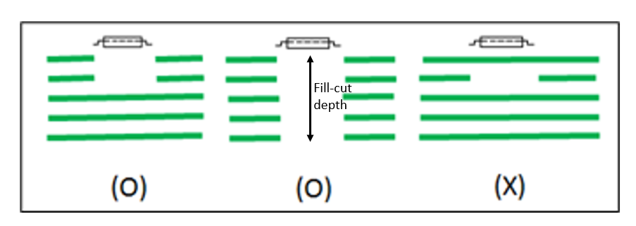
- Minimum fill-cut distance: Set minimum distance between component's pad and fill-cut.
- Fill-cut depth: Set the depth of fill-cut by number. DFE checks up to "Fill-cut depth +1" layer. If there is no fill-cut within the "Fill-cut depth", it is reported as a failure. If a fill-cut exists on the "Fill-cut depth+1" layer, it is also reported as a failure.
- Measure Base: Select Pad base or Pad pair base of passive component.
- Additional passive component: This option to select additional composite passive component.
- Check Range: Set the range between start component and end component.
- Start Component: Select start component to measure range.
- End Component: Select end component to measure range.
- Exception Options
- Pin Escape: Enter a radius of circular region around pins to be excluded for the rule check.
- VIA Escape: Enter a radius of circular region around vias to be excluded for the rule check.
- Exclude Serpentine Area: DFE does not check serpentine section of net.
- Exclude Arc are: DFE does not check ARC section of net.
- Exclude Short Segment Error: Exclude the short length trace shorter than this value.
- Display Separation & TP Distance Result: PollEx DFE report will show segment/TP separation information.
- Use Edge-to-Edge Separation: Checks edge-to-edge separation.
Default: Center-to-Center
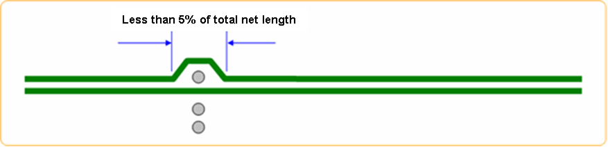
Figure 5.
To design a Differential Pair Net, you must pay attention to keep the continuity of power and ground planes above and below of the differential net. Do not make branch stub to make test point. In other words, impedance for overall routing must be kept the same for the pair nets.
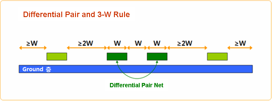
Figure 6.
Reference Material
Parallelism will cause impedance discontinuities that will directly affect signal quality.
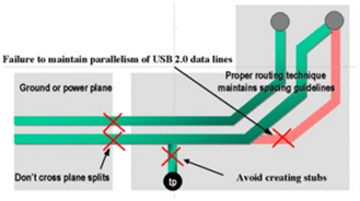
Figure 7.
- Intel - High Speed USB Platform Design Guidelines