Electrical Pins
Define the shape and properties of electrical pins.
-
Click Properties > Electrical Pins.
The Electrical Pin dialog opens.
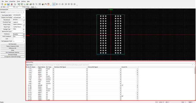
Figure 1. -
Signal Data: Display the general data of the electrical pins.
- Pin No.: Display the pin number (not editable).
- Pin Name: Display the pin name (not editable).
- Signal Name: Display the signal name of the pin. This name is editable.
- Pin Type: Display the pin type. User can define the pin type depending on the characteristic of the pin.
- Pull-down Ref Signal: Define the pull-down reference signal name of the pin.
- Pull-up Ref Signal: Define the pull up reference signal name of the pin.
- Invert Pin: Define the invert pin of the pin.
-
Driver/Receiver Model Data: Click the Driver/Receiver Model
Data tab.
-
Model Type: Define the device model type of the pin.
IBIS, SPICE, HSPICE and LINEAR models are available.
- Model File: Select the device model file of the pin.
- Driver Model: Select the driver model of the pin.
- Receiver Model: Select the receiver model of the pin.
-
Model Type: Define the device model type of the pin.
-
Package Pin Parasitic Model Data: Click the Package Pin Parasitic
Model Data tab.
-
Model Type: Define the package pin parasitic model type of the pin.
Lumped, Distributed, S-parameter and SPICE models are available.
-
Model File: Select the package pin parasitic model file of the
pin.
Resistance/Inductance/Capacitance: These properties are automatically by the device model file and you can edit the properties.
-
Model Type: Define the package pin parasitic model type of the pin.
-
Attribute: Click the Attribute tab.
-
Attribute: Show and edit attribute.
- Add: Add a new attribute.
- Remove: Remove the selected attribute.
- Edit: Edit the selected attribute.
-
Attribute: Show and edit attribute.