Analyze Net Topology
After finishing net topology construction and assigning a simulation model, analyze net topology using the Net Topology Analyzer.
-
Use the Net Topology Analyzer dialog to analyze
interconnect network of individual nets in time and frequency domains to obtain
the transient waveforms, eye diagrams, and frequency-dependent network
parameters which are different views of the signal delay and distortion.
When a differential net is selected, both differential pair nets are included in the same network analysis model.
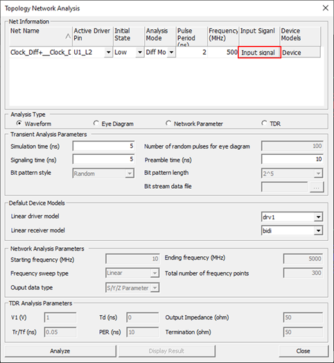
Figure 1.When multiple output or bi-directional pins are available for the net, one of them must be selected for active driver pin. The pulse initial state and period of input signal is automatically obtained from the operating frequency of the net. Clicking Input Signal allows you to view the input signal property and change them. After checking Define Pulse Data you can also change the high/low state of each bit of the input signal.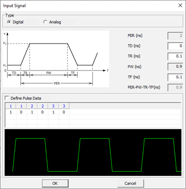
Figure 2.Click Device Models to view the device models selected for the output and input pins. You can change the device model selection when multiple models are available for the pin.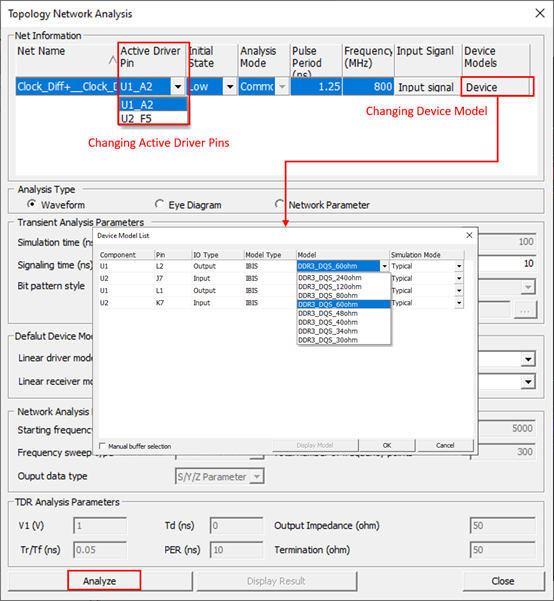
Figure 3.Prior to running analysis, you need to select an analysis type and make necessary changes on the analysis control parameters. Waveform, Eye Diagram, and Network Parameter are the available analysis types. Analysis run control parameters vary with the analysis type and are initialized with the ones shown in Electrical Analysis Constraints menu.
Waveform analysis is running transient circuit simulation on the network model for you-specified simulation time in order to obtain time-domain voltage waveforms at the input and output nodes. Signaling time refers how long the driver pin keeps transmitting signals. To see the waveforms after the driver pin becomes inactive, the simulation time should be longer than the signaling time plus the signal delay of the input signal.
The analysis is performed upon selecting Analyze menu. Upon completion of the analysis, waveforms at all input and output nodes are displayed. You can also view the measurement voltage (Vmeas), input signal (*_in), and enable signal (*-en) of each output pin as well as static overshoot voltage high (Vmax), static overshoot voltage low (Vmin), logic threshold voltage high (Vinh), and logic threshold voltage low (Vinl) of each input pin. For differential nets, you can view the waveforms of voltage differences (Vdiff) between the differential input node pairs by selecting them which are shown under the positive input nodes. Selecting or unselecting an input node for waveform display makes the differential pair node be automatically selected or unselected. Many displays and measuring options are available in the Viewer Option. The analysis results can be listed in a table form by clicking Result Data tab. They can be also shown in MS Excel. The waveform data can be saved in a file with the use of Save or Save As menu. Save menu saves the file in Signal_Integrity/Waveform directory under the design job folder. The model name plus .spw is used for the file name. The saved waveform data can be read into the waveform viewer alone or together with other waveform data for a review or comparison.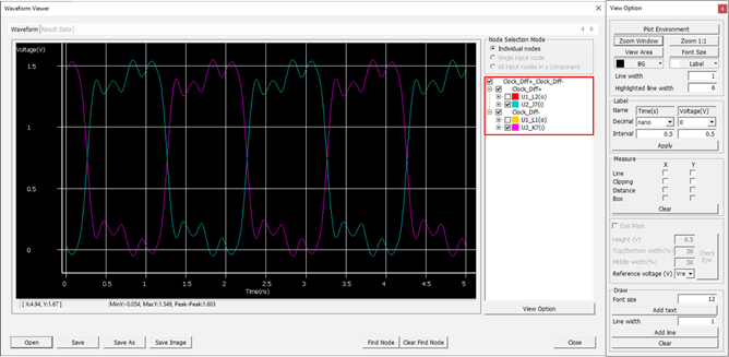
Figure 4.Eye Diagram analysis is running transient circuit simulation on the network model to obtain eye diagrams at the input nodes. An eye diagram or eye pattern is obtained from overlapping multiple waveforms at the receiver node of a net generated by randomly selected high/low states of the input signals for the selected net and adjacent nets. The coupling effects from the adjacent nets are reflected in the waveforms. Prior to running analysis, you can change the analysis control parameters such as the number of random pulses and bit pattern style.
Upon completion of the analysis, the eye diagrams at input nodes are displayed in the waveform viewer. Check Eye menu allows you to check if the eye size is large enough with the use of eye mask. The height and width values of the eye mask are initialized with the ones defined for the net, and you can change them. Among many available display and measurement options, Box can be effectively used for measuring the eye size. With X box checked you can make a rectangular box by placing two vertical lines. The eye mask height is used for the box height. On the other hand, with Y box checked you can make a rectangular box by placing two horizontal lines. The eye mask width is used for the box width. The eye diagram waveform data can be saved in a file with the use of Save or Save As menu. Save menu saves the file in Signal_Integrity/Waveform directory under the PCB design job folder. The model name plus .spe is used for the file name. The saved eye diagram waveform data can be read into the waveform viewer alone or together with other eye diagram waveform data.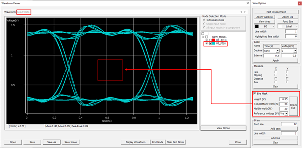
Figure 5.Network Parameter analysis is running AC circuit simulation on the interconnect network model to obtain network parameters between the ports in the model. A port is assigned to each pin location. The analysis results include the scattering (S), admittance (Y), and impedance (Z) parameter matrices at each frequency point. Prior to running analysis, you can change the analysis control parameters such as the starting and ending frequency points, frequency sweep type, and number of frequency points for the sweep type.
Upon completion of the analysis, the S-parameter magnitude values among ports are initially displayed in the network parameter viewer. You can change the port pair selections and change the value type to decibel, phase, real number, or imaginary number. You can choose the network parameter type for the display among S-parameter, Y-parameter, and Z-parameter. Many display and measurement options are available in the network parameter viewer. Result Data menu is used to list the network parameter values in a table format. The network parameter values can be saved in a Touchstone format file. Additionally, they can be viewed in MS Excel.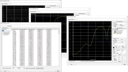
Figure 6.You can select multiple network analysis models for analysis. The selected models are analyzed one by one, and the analysis results are displayed together. The network models with analysis results are saved in Signal_Integrity/NWK directory under the PCB design job folder by selecting Save menu. The model name plus .NWK is used for the file name. The saved models are listed in the left-hand side of the window. You can select the saved models anytime and copy the model to view the model, view the analysis results, edit the model, and rerun analysis.
Analysis > Network Analysis menu enables you to execute three different types of analysis mentioned above. The output waveform is influenced by the signal delay and reflections of the selected net(s) but not by the crosstalk from the neighboring nets.
Waveform Analysis: EM simulation will give SPICE netlist for the topology and Spice source will be applied to it to do the transient analysis. Time domain voltage waveforms for the driver/receiver pins connected to the topology will be displayed automatically after the SPICE analysis done.
Eye Diagram: Random bits sequence will be applied to the selected net(s) and the eye diagram which shows the quality of the transmitted signals (bits) passing through it will be displayed repeatedly over the specified Pulse Period.
Network Parameter: Extracts S, Y and Z parameters for the selected traces. Using Network Parameter Viewer, you can investigate the parameters in both graphic and table data format. S parameter can be exported as “touch stone file”.
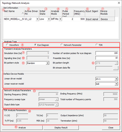
Figure 7.- Net Name: All selected net names will be listed.
- Active Driver: You can specify the active driver pin among the connected pin to this net. The other pins will be assigned as receiver pin(s) automatically.
- Initial State: You can specify the initial value of input waveform.
- Analysis Mode: You can select the signal to assert the mode of the differential pair net. (Differential Mode/Common Mode)
- Pulse Period/Frequency: You can adjust the driver’s operating frequency/speed by changing this value.
- Input Signal: Double-click Input signal to change the detailed
parameters which can specify the actual shape of the input signal, for
example: TD (Time Delay), TR (Rise Time), TR (Fall Time), and PW (Pulse
Width).
Figure 8. - Device Models: For the selected active driver, actual driver model can
be selectable among many different models in IBIS or Linear device model
types. You can use one of available models considering the output
impedance, driving capability measured by output current level and
operating frequencies. These driver’s characteristics lead huge impact
on the simulated waveforms.
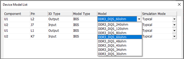
Figure 9. - Analysis Type: Just click the one of desired analysis type. And then editable setting parameters will be shown.
- Simulation time: End time of the SPICE transient analysis.
- Signaling time: Input Signal having pulse period as (2ns) will be excited to the net until the time assigned here.
- Bit pattern style: When you select the Eye diagram analysis, you can change the random bit generation algorithms among ABS, random and PRBS.
- Bit pattern length: Total number of random bits will be applied to the net.
- Network Analysis Parameters: Specify the start and end frequencies,
total number of frequency points and the method of sweeping the
frequency points.
- Linear: Network parameter will be solved for “50” frequency
points between 1 MHz ~ 5000 MHz.
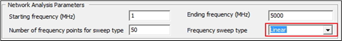
Figure 10. - Decade: Network parameter will be solved for “150” frequency
points, 50 points from 1MHz ~ 10MHz, 10MHz~100MHz and
100MHz~1000MHz respectively.
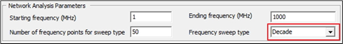
Figure 11.
- Linear: Network parameter will be solved for “50” frequency
points between 1 MHz ~ 5000 MHz.
- TDR : The parameters for TDR analysis are as follows.
- V0: Square wave voltage output from the driver stage.
- Tr/Tf(ns): Rising/Falling time of square wave output from Driver.
- Td(ns): The initial delay time of the square wave output from the driver stage.
- PER(ns): The period of the square wave output from the driver stage.
- Output Impedance(ohm): The output impedance of the driver.
- Termination (ohm): The termination Impedance.
- Analyze : Three types of simulation will be started by this button.