Transmission Line Analysis
In many cases, you want to know the characteristic impedance of the traces on a certain layer depending on the user defined thickness and width of it. Or user may want to get optimized trace width and distance values over specific layers which having certain targeted characteristic impedance.
Traces used for routing nets are modeled as transmission lines. Transmission Line Analysis menu is used to run transmission line analysis to extract parasitic parameters and line characteristics of single and multi-conductor trace models or to find impedance matching trace configurations to minimize the signal integrity problems. A built-in full-wave electromagnetic field solver is employed for the transmission line analysis. This function can be effectively used at a pre-design stage for optimizing the board layer stack-up and determining the trace widths to use for routing nets.
Creating a transmission line model starts with entering the model name and selecting the analysis type among Extract Trace Parasitic Parameters and Get Impedance Matching Trace.
Extract Trace Parasitic Parameters
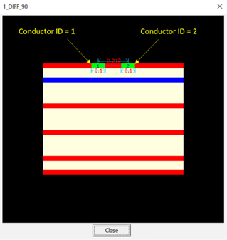
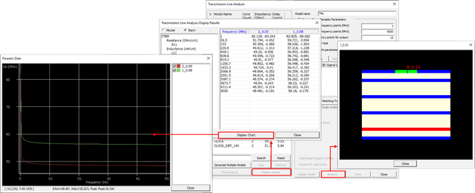
For extracting frequency-dependent parasitic parameters of the model, users can change the analysis control parameters such as lower and upper bounds of frequency points, number of frequency points for output, and frequency sweep type. Add Conductor menu is used to add conductor or ground traces to the model. For each trace (conductor), users need to select the conductor type (Conductor or Ground) and signal layer and define the conductor width and location. Display Model menu is used to graphically display the transmission line model.
Retrieve Impedance Matching Traces
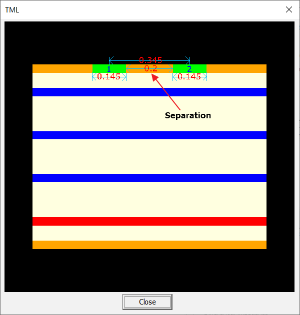
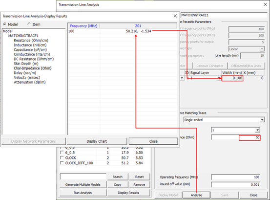
Getting trace configuration with characteristic impedance matching the user-defined target impedance value at the operating frequency starts with selecting the signal type among Single-ended, Differential narrow, Differential broad, and Shielded. For single-ended signal trace, you must select the signal layer and specify the target impedance to obtain the impedance matching trace width. For narrow-side differential signal trace pair, you must select the signal layer and specify the target differential impedance. Either the trace width or separation between the trace pair must also be specified. With known trace width the trace separation value is obtained. On the other hand, with known trace separation the trace width is obtained. For broad-side differential signal trace pair, you must select two adjacent signal layers and specify the target differential impedance. Assuming the widths of the differential trace pair are identical, the trace width is obtained. Shielded signal type represents a signal trace surrounded by ground traces at both sides. For the shield signal trace, users are required to select the signal layer and specify the ground trace width and target impedance. Either the signal trace width or separation between the signal trace and ground traces must also be specified. With known signal trace width, the trace separation value is obtained. On the other hand, with known trace separation the signal trace width is obtained.
Upon selecting the Analyze menu, the impedance matching transmission line model is automatically found by iteratively running the electromagnetic field solver. Then the analysis results at the operating frequency point are displayed. Upon completion of the analysis, the analysis type is automatically switched to Extract Trace Parasitic Parameters for the impedance matching transmission line model. The model can be graphically viewed in Display Model menu.
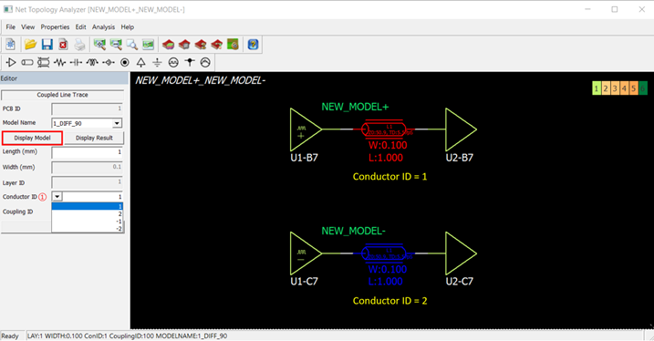
The transmission line model with analysis results is saved in Signal_Integrity/TML directory under the PCB design job folder by selecting the save menu. The model name plus .TML is used for the file name. The saved models are listed in the left-hand side of the dialog. You can select the saved models anytime to view the analysis results and copy the model to view the model, edit the model, and rerun analysis. Additionally, the saved transmission line models are shared with Net Topology Analyzer, which allows the models to be used for net topology analysis.