Edit Properties

  1. Edit materials.
    1. From the menu bar, select Properties > Materials.
      The Material Manager lists the default material list used by PollEx PI.
    2. Add. modify, remove, or export materials as material files (*.mtrl) from this dialog.
    3. Double-click on a material to change its properties.
  2. View PCB's physical stacked information used for power integrity analysis.
    1. From the menu bar, select Properties > Layer Stack.
      The Layer Stacks window shows PCB's stacked information. The stacking order, thicknesses and material properties of metallic and dielectric layers are core parameters drawing dramatic changes of signal transmission qualities and thermal distribution over PCB systems. Therefore, precise assignment should be given to Type, Thickness, Conductor/Dielectric Material, and the total thickness should be checked whether it shows proper value.
  3. View part property assignment.
    1. From the menu bar, select Properties > Parts.
      • The Parts dialog shows the status of the properties assignment to the parts which are included in the current PCB system to analyze. Function Type and Cost of each component are editable from this dialog.
      • The Parts dialog shows also the Model Type, Model File and Model Name if there is part assigning with SPICE or S-Parameter model.
      • If you click the Update Part Information, you can load and apply the currently configured part information.
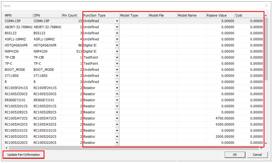

      Figure 1.
  4. From the menu bar, select Properties > Via Padstacks to view pad-stack information used in the design.
    You cannot modify the parameters from this dialog.
  5. Select Properties > Signal Nets to view selected signal net information.
    You cannot modify the information from this dialog.
  6. Select Properties > Power Ground Nets to view target power and ground net information.
    You cannot modify the information from this dialog.
  7. Select Properties > Output Components to view receiver component information.
    You can edit the Placed Layer from this dialog.
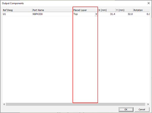

    Figure 2.
  8. Select Properties > VRMs to view power source component information.
    You can edit the Placed Layer and also RLC values from this dialog.
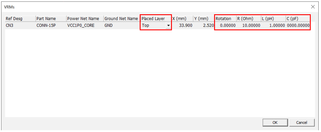

    Figure 3.
  9. Select Properties > Ports to view power load component information.
    You can :
    • choose each port you want to use on this dialog
    • edit the DC Current (mA) for DC IR-Drop analysis from this dialog
    • edit the R (ohm), L(nH) and C(pF) value for each ports
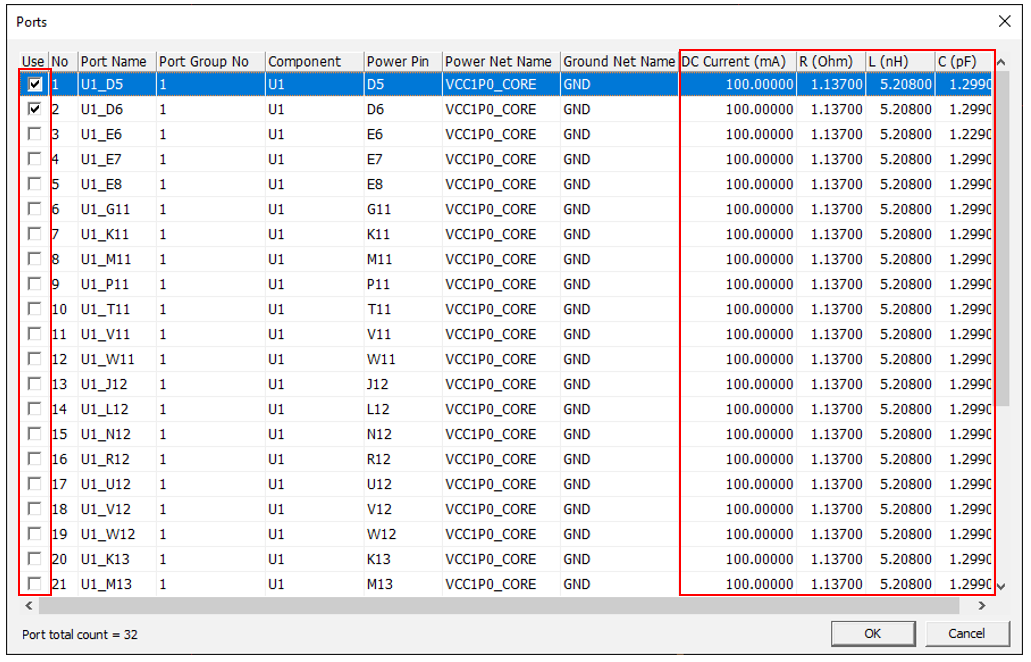

    Figure 4.
  10. Select Properties > Decoupling Capacitors to view current test case and capacitor information.
    • Add Case: Add the new test case. The test case applies only to PDN analysis.
    • Copy Case: Add the new test case while maintaining the capacitor information of selected test case.
    • Remove Case: Remove selected test case.
    • Assign Decaps: Assign a value to the selected capacitor. Upon clicking this menu, the Assign Decaps dialog opens. By clicking required capacitor, the capacitor value will be changed.
    • Show Decap Location Property: Open the Decap Location Property dialog which displays whole capacitor information.
  11. Select Properties > Composite Passive Components to view composite passive components connected to the selected power net (Exclude Capacitors).
    You can calculate Effective Resistance if there is composite passive component which is importing S-parameter data from this dialog.
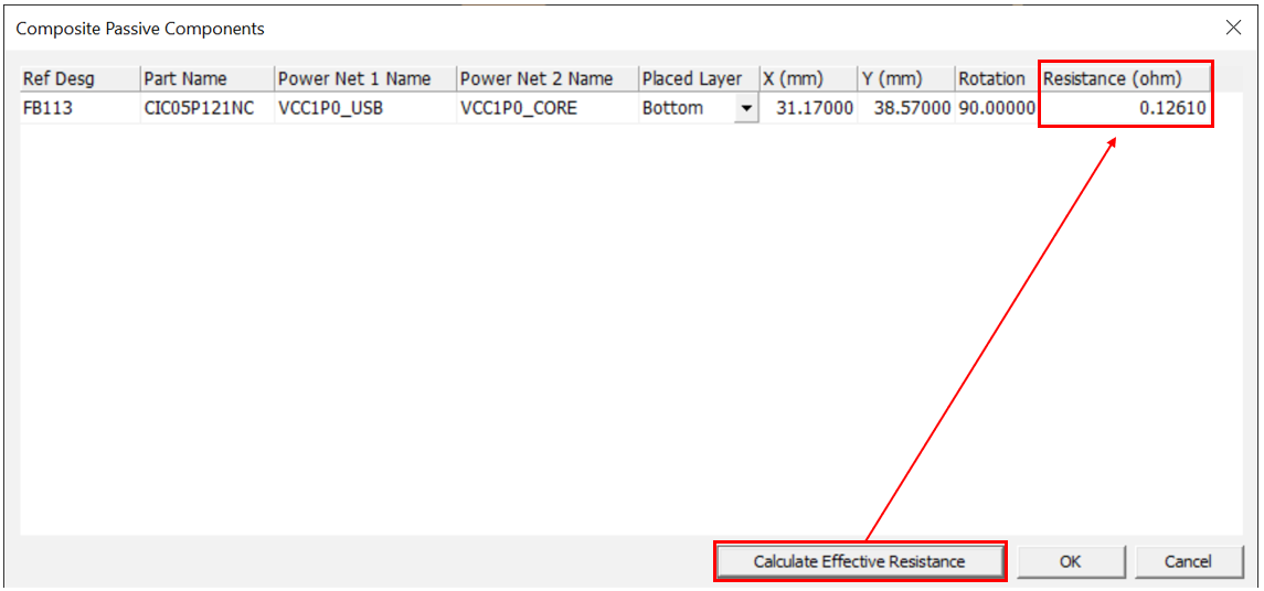

    Figure 5.