Direct Generation - Mounting Data Setting
create mount data directly through the Mounting Emulator.
Global parameters:
- Mount Type: Chooses mounter type to export mount data.
- Import BOM: This option used for referring BOM to export mount data.
- BOM File Path: Defines BOM file.
- BOM Setting File (*.EBI) Path: Defines the environment file (*.EBI) of PollEx BOM to export formatted Excel file.
- Define Part List Column Name: If not using the environment file (*.EBI) of PollEx BOM, you can set each column to export the formatted Excel file.
- Mounting Library: Can create mount data by referring to the Mounting Part
Code Table when the part code used in the mounter is different from the part
data used in the PCB data and BOM.
- Mounting Library File Path: Sets the file path of mounting library that is the Part Code used in the mounter, and the Part Code Matching Table file used in the PCB and BOM.
- Set Mounting Part Code: Can search by part code or edit the part information in Mounting Library Mapping Table.
- Property Value Matching: Part information that matches both the Property Value and Part Name on the PCB design data is recognized from the Mounting Part Code Table.
- Decimal Place: Set the decimal place when generating mounting coordinate data. Select a value from 1 to 5.
Board Parameters
- Board Size: Can check the size information of the board and set the
thickness.
- Width(X): The size of the board in the horizontal direction.
- Height(Y): The size of the board in the vertical direction.
- Thickness(Z): Can set the board thickness.
- Origin Offset: Set X and Y offset value of board origin.
- Board Origin Location: Sets the location of board origin.
- User Defined Origin: Selecting this option allows you to set the origin position directly.
- Set nearest sub board from board origin as block data: Sets the block data by nearest sub board from the selected board origin.
- Generate block data only: Can export only block data when exports mount data.
- Carrier JIG Definition: If Carrier JIG was used, can set the size of Carrier
JIG and set the X and Y offset value from Carrier JIG to board.
- Width(X): Sets the size of Carrier JIG in the horizontal direction.
- Height(Y): Sets the size of Carrier JIG in the vertical direction.
- Carrier JIG Offset from Board Origin: Can set the X and Y offset value from Carrier JIG to board.
- Array: Sets the information of arrayed board.
- Horizontal Count: Enters the number of sub boards on the horizontal axis.
- Vertical Count: Enters the number of sub boards on the vertical axis.
- Apply Array Coordinate from Design: After entering the number of sub boards in Horizontal/Vertical Count then clicking this button, the input item is activated as much as the number of sub boards in the array table. Enter X, Y and Angle values for each sub board.
Component Parameters
- PoP Component Definition: For parts with high component densities, such as
mobile phones and digital cameras, a package on package (PoP) design is
sometimes applied. Option to check if the position of pin 1 of the upper
part of the PoP is the same as the position of pin 1 of the lower part.
- Filter: Sets through the string filter to recognize the top part of
the POP from the mounting data.
Figure 1. 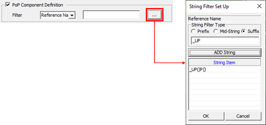
- In the above example, the part with the same reference name and the suffix _UP is recognized as the top material of the PoP. For example, if U100 and U100_UP exist in the mounting data, U100 is recognized as lower part and U100_UP as upper part.
- Filter: Sets through the string filter to recognize the top part of
the POP from the mounting data.
- Except Component: It is an option to exclude certain parts in PCB design that are not target components, such as Test Point, Screw, Fiducial Mark, and so on, when exporting mount data. Set it using the part DB file (*.txt) file.
- Allowable Component with the Rotated 180 Degrees: Can allow for a 180-degree
mounting angle for not having polarity mark.
- Use UPF Option (Rotated 180 Degrees): If Allow Reverse (180) option is checked on the Mount Data of the UPF 3D Parts Library, it is an option that allows 180 degrees of distortion.
- Define Component List Path: Allows 180-degree distortion for parts corresponding to the specified Component DB (*.txt) file.
- Export Component Angle as 0 or 90 Degrees: Can export 0 degrees in the horizontal direction and 90 degrees in the vertical direction for parts corresponding to the designated Component DB (*.txt) file.
Fiducial Mark Parameters
- Fiducial Mark: Sets the location and shape information of fiducial mark on
board placed.
- Name: Enters the name of fiducial mark.
- X: Enters the X coordinate of fiducial mark.
- Y: Enters the Y coordinate of fiducial mark.
- Shape: Chooses the shape of fiducial mark as circle or rectangle.
- Locate: Sets directly fiducial mark by selecting on PCB design or by
entering the coordinate.
- X: Means X coordinate of fiducial mark.
- Y: Means Y coordinate of fiducial mark.
- Locate: Displays the location to the screen by using X and Y coordinate values.
- Object Picking: If fiducial mark is registered as a part, selecting the part can get the X and Y coordinates of the fiducial mark.
- Location: If selects the location of fiducial mark on PCB directly, can get X and Y coordinates of the fiducial mark.
- Add Fiducial Mark: Clicks this button, can add more list into Fiducial Mark List Table.
- Fiducial Light: Set the lighting value for fiducial mark recognition on the mounter.
- IC Fiducial Mark Definition: Sets the IC fiducial mark information like size
and location.
- Component: If the IC Fiducial Mark is designed as a part on the PCB design, it can be recognized using a string filter. Selects string filter conditions from reference name, part name, footprint name, and package name.
- String Filter: Selects type of string filter from prefix,
mid-String, suffix, and input the string for part recognition. The
example below means that the part name on the PCB design recognizes
all parts starting with IC_FID.
Figure 2. 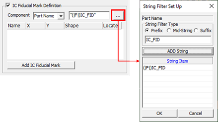
- Table: When directly registering IC fiducial mark, click
Add IC Fiducial Mark and enter it
directly into the table.
- Name: Enters the name of IC fiducial mark.
- X: Enters the X coordinate of IC fiducial mark.
- Y: Enters the Y coordinate of IC fiducial mark.
- Shape: Chooses the shape of IC fiducial mark as circle or rectangle.
- Locate: Directly sets IC fiducial mark by selecting on PCB design or by entering the coordinate.
- X: Means X coordinate of IC fiducial mark.
- Y: Means Y coordinate of IC fiducial mark.
- Locate: Displays the location to the screen by using X and Y coordinate values.
- Object Picking: If the IC fiducial mark is registered as a part, the X/Y coordinates of the IC Fiducial Mark are entered when the part is selected.
- Location: If selects location of IC fiducial mark directly on PCB design, the X/Y coordinates of it are entered when the location is selected.
- Add IC Fiducial Mark: Add more list into IC Fiducial Mark List Table.
- Bad Mark Definition: Sets the shape and location of bad mark.
- Component: When bad mark is designed as a part on PCB design, it can be recognized by using string filter. Select string filter conditions from reference name, part name, footprint name, and package name.
- String Filter: Selects the string filter type from prefix,
mid-string, and suffix, and enter the string for part recognition.
The example below means that the part name on the PCB design data
recognizes all parts starting with MARK_BAD.
Figure 3. 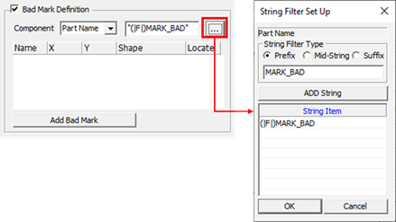
- Table: Can add and define bad mark. Clicks Add Bad Mark button and
enter the information.
- Name: Enters the name of bad mark.
- X: Enters the X coordinate of bad mark.
- Y: Enters the Y coordinate of bad mark.
- Shape: Chooses the shape of bad mark as circle or rectangle.
- Locate: Sets directly bad mark by selecting on PCB design or by entering the coordinate.
- X: Means X coordinate of bad mark.
- Y: Means Y coordinate of bad mark.
- Locate: Displays the location to the screen by using X and Y coordinate values.
- Object Picking: If the bad mark is registered as a part, the X/Y coordinates of the bad mark are entered when the part is selected.
- Location: If selects location of bad mark directly on PCB design, the X/Y coordinates of it are entered when the location is selected.
- Add Bad Mark: Add more list into Bad Mark List Table.