Creating the Model

Create the model in CADFEKO. Define any ports and sources required for the model. Specify the operating frequency or frequency range for the model.

  1. Set the model unit to millimeters.
  2. Define the following variables:
    • d = 5.8 (The spacing for the periodic boundary condition.)
    • h = 0.5 (The thickness of the substrate.)
    • t = 0.091 (The thickness of the bonding material.)
    • s1 = 0.15 (The width of the dielectric surface, bottom layer.)
    • s2 = 0.18 (The width of the dielectric surface, upper layer.)
    • w = 2.5 (The width of the centre metallic surface.)
    • fmin = 5e9 (The minimum frequency.)
    • fmax = 15e9 (The maximum frequency.)
  3. Create the two dielectric media.
    1. Create the dielectric medium, Dielectric1.
      • Relative permittivity: 3.38
      • Dielectric loss tangent: 0
      • Label: Dielectric1
    2. Create the dielectric medium, Glue.
      • Relative permittivity: 3.3
      • Dielectric loss tangent: 0
      • Label: Glue
  4. Create a cross shape.
    • Arm length (Lu): d/2
    • Arm length (Lv): d/2
    • Strip width: w
    • Label: Cross
  5. Create a plane shape for the bottom layer.
    • Width (W): d-s2
    • Depth (D): d-s2
    • Label: Plane_Bot
  6. Create a plane shape for the top layer.
    • Width (W): d-s1
    • Depth (D): d-s1
    • Label: Plane_Top
  7. Create a unit cell.
    1. In the Reference vector drop-down list select U vector.
    2. Dimensions:
      • Skew angle θ : 0.0
      • Distance (U): d
      • Distance (V): d
    3. Create the following layers:
      Layer 1:
      • Method: Select Metal in the drop-down list
      • Shape: Select Plane_Top in the drop-down list
      • Rotation: 0
      • OffsetU: d/2
      • OffsetV: d/2
      Layer 2:
      • Method: Select Substrate in the drop-down list
      • Medium: Select Dielectric1 in the drop-down list
      • Thickness: h
      Layer 3:
      • Method: Select Metal in the drop-down list
      • Shape: Select Cross in the drop-down list
      • Rotation: 0
      • OffsetU: d/2
      • OffsetV: d/2
      Layer 4:
      • Method: Select Substrate in the drop-down list
      • Medium: Select Glue in the drop-down list
      • Thickness: t
      Layer 5:
      • Method: Select Substrate in the drop-down list
      • Medium: Select Dielectric1 in the drop-down list
      • Thickness: h
      Layer 6:
      • Method: Select Metal in the drop-down list
      • Shape: Select Plane_Bot in the drop-down list
      • Rotation: 0
      • OffsetU: d/2
      • OffsetV: d/2
    4. Z value at the top of layer 1: 0
    5. Label: UnitCell1
  8. Select the UnitCell1 (under the Unit Cells group) and click Build Geometry
    1. On the dialog, select the Set Periodic Boundary Condition (PBC) checkbox.


    Figure 1. Top view of the FSS after building the geometry of the unit cell
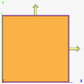
    Note: To visualise the periodic nature of the geometry, make a copy of the built geometry part (UnitCell1) in the X direction. Then copy both geometry parts in the model tree in the Y direction.
  9. Add a single incident plane wave with θ=0° and ϕ=0°.
  10. Set a continuous frequency range from fmin to fmax.