Silk on Pad
Check if silkscreen data are overlapped with pads.
- Silkscreen Definition: Define silkscreen layers for top and bottom layer.
- Top: Select silkscreen top layer from layer list.
- Bottom: Select silkscreen bottom layer from layer list.
- Using Gerber Layers: If users want to use silkscreen as GERBER file
in checking, define silkscreen GERBER top and bottom layer, respectively.
- Top Silk Layer: Select silkscreen GERBER top layer.
- Bottom Silk Layer: Select silkscreen GERBER bottom layer.
- Target Component Definition: Define target components.
- All Components: All components on board will be target components.
- Exclude Components: Among whole components on board, select void-checking components by selecting component groups.
- Component Group Selection: Select target components by selecting component groups.
- All Components: All components on board will be target components.
- Target Silkscreen Objects Definition
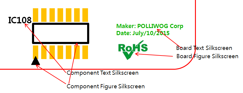
Figure 1. 
- Pads Objects: Checks pads overlapping with silkscreen data in below list.
- Component Text: Check pads overlapping with component text silkscreen.
- Board Text: Check pads overlapping with board text silkscreen.
- Component Figure: Check pads overlapping with component figure silkscreen.
- Board Figure: Check pads overlapping with board figure silkscreen.
- Vias Objects: Checks vias overlapping with silkscreen data in below
list.
- Component Text: Check vias overlapping with component text silkscreen.
- Board Text: Check vias overlapping with board text silkscreen.
- Component Figure: Check vias overlapping with component figure silkscreen.
- Board Figure: Check vias overlapping with board figure silkscreen.
- Except for Silkscreen with Zero width: Exclude from the inspection if the width of the silk object is 0.
- Pads Objects: Checks pads overlapping with silkscreen data in below list.
- Checking
- Clearance between Silkscreen and Target Objects: Check the clearance
between silkscreen and selected objects. To do checking for this,
set the clearance value.
- Measure Base for Pads: Select measure base for pads.
- PAD: Measure based on the Pad shape.
- Solder Mask: Measure based on the Solder Mask shape.
- Pad/Solder Mask Overlap: Measure based on the area where the Pad and the Solder Mask of component overlap.
- Measure Base for Pads: Select measure base for pads.
- Measure Base for Vias: Select measure base for Vias.
- PAD: Measure based on the Pad shape.
- Solder Mask: Measure based on the Solder Mask shape.
- Pad/Solder Mask Overlap: Measure based on the area where the Via’s pad and the shape of the Solder Mask overlap.
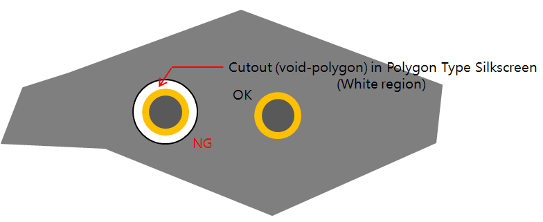
- Finding Via Cutouts for Polygon Type Silkscreen: If the silkscreen
is composed with polygon, there should not be inner void polygon.
PollEx DFM detects it.
Figure 2. 
- Clearance between Silkscreen and Target Objects: Check the clearance
between silkscreen and selected objects. To do checking for this,
set the clearance value.