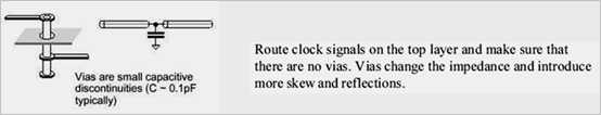
This item checks layers change by counting the number of Vias used in a signal
net.
Some of the signal traces have special characteristics so that they are not allowed
to change layers. For the impedance controlling net, layer change is a critical
element for impedance shift. In order to prevent impedance shifts, the designer
restricts the change of trace width and the change of layers to minimize
possibilities of problems.
Check the number of vias used in signal net
Item: Input item name.
Net: Select a target net group.
Limit: Select via quantify check type between Min and Max.
Via Qty: Assign the number of vias allowed in a net or nets for the
target net group.
Composite Power Net: DFE uses composited power net instead of single
power net. Double-click the item field. The Composite
Power Net dialog displays.
Passive Comp Group: The DFE makes composite net which are
connected through this passive component.
Exception Net Group: Nets that should not be merged into the
composite net.
Start Component: When multiple load components exist, the tool
checks via count for each path to load component.
Check the number of vias used in signal net copper area.
Via Qty On Copper: Check via quantity of copper area if net has
copper area.
Check pad on via quantity of pin pad which are connected to selected signal net.
Connected Comp: Select component check pad on via quantity of ground
pin pad.
GND Net: Assign Ground signal group in order to determine GND pin of
component.
Pad on Via Qty(Min): Assign the number of minimum via should be
exist on ground pad.
Expand Pad Area: The maximum distance between pad and via.
Composite Power Net: DFE uses composited power net instead of single
power net.
Composite Power Net:
Passive Comp: The DFE makes composite net which are
connected through this passive component.
Exception Net: Nets which should not be merged into
composite net.
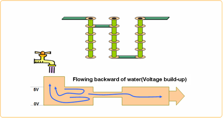
In high speed signal, via can make impedance mismatching and result in generating
crosstalk. This symptom causes a voltage rise. Therefore, it is recommended to use a
limited number of vias.Figure 1.
Figure 2.
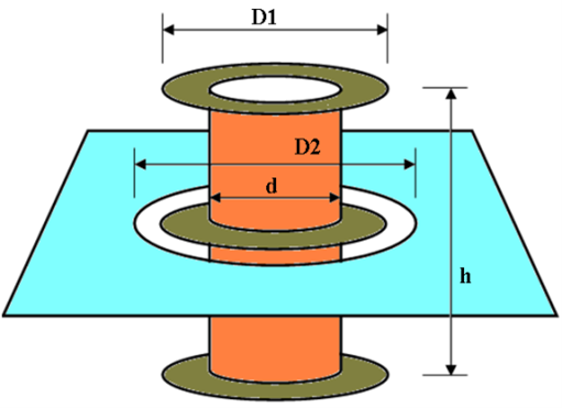
Capacitance of Vias
Figure 3.
Where,
Diameter of hole in ground planes, in.
Diameter of via pad, in.
Thickness of PCB or dielectric, in.
Relative dielectric constant of PCB material.
Parasitic via capacitance, pF.
Minimize by:
Reducing capture pads.
Eliminating NFPs (non-functional pads).
Increasing anti-pads.
Inductance of Vias
Where,
Length of via, in.
Diameter of via, in.
Inductance of via, nH.
Minimize by:
Eliminating and/or reducing stubs.
Minimizing via barrel length by routing outer layers near surface layers and
applying Back drilling to remove the parasitic stub.