This rule checks whether nets keep allowable trace widths.
In analog design, signal impedance is not an important factor in routing and signal
trace widths are decided depending on allowable current values. Assuming PCB layer
thickness remains the same, trace width is a main factor in deciding current
carrying capability of the trace.
Item: Input item name.
Net: Select a target net group.
Limit: Select allowable value type between Min, Max and Middle.
Tolerance(%): Input allowable trace width ratio relative to the Limit
Width.
Limit Width: Assign a reference trace width (Limit Width).
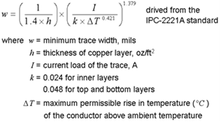
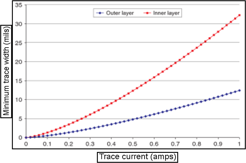
Trace Width and Current Carrying Capacity
When current flows through a conductor, it will heat up due to I2R losses. Larger
cross section (for example, wider and/or thicker) traces exhibit less resistance and
therefore less heating.
To determine the minimum trace width required to minimize heating, determine the
maximum current a trace will carry and the thickness of the copper you will use on
PCB.
The minimum trace width is expressed as:Figure 1. Figure 2.
(Derived from the IPC-2221A standard)
Where,
Minimum trace width, mils.
Thickness of copper layer, oz/ft2.
Current load of the trace, A.
0.024 for inner layers.
0.048 for top and bottom layers.
Maximum permissible rise in temperature (Celcius) of the conductor above
ambient temperature.