3D Clearance
This item helps you figure out how far apart two objects should be on a PCB. It considers the PCB's thickness and calculates the minimum space needed between objects placed on the top and bottom layers of the PCB. Because PCBs are composed of multiple layers, the distances and spaces between these layers have an impact on signal quality and stability. For example, 3D clearance prevents signal routes, power delivery networks, and component conflicts at each layer of the PCB, ensuring electrical reliability. This technology minimizes interference between signals/components and helps to prevent electrical issues before PCB manufacturing. Therefore, through 3D clearance checks, considering PCB thickness, one can efficiently manage interference between signals/components, enhancing system stability.
- Item: Input item name.
- Check Type: Select whether to check the distance between two nets or the distance between the net and the component.
- Object: Select the two objects (components or nets) to be measured for the 3D clearance, Object1 and Object2.
- Clearance: Enter the minimum clearance distance the user wishes to inspect,
and note that the user cannot input alphabetic or negative values.
Figure 1. 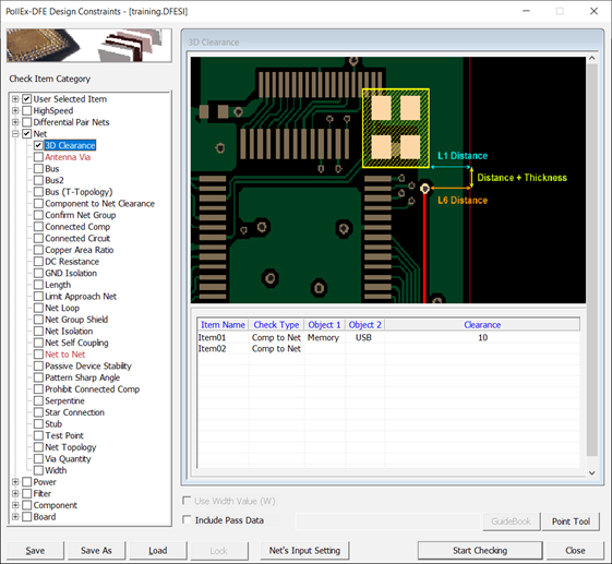
The following shows three distances of the 3D clearance:Figure 2. 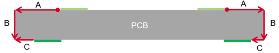
- A - how close an object is to the PCB's edge on the top layer.
- B - the thickness of the PCB itself.
- C - how close an object is to the PCB's edge on the bottom layer.
It then calculates the shortest distance for either the top or bottom layer automatically. This feature helps users check if the design between two targets on their PCB is safe in terms of the 3D space they need.