This DFE rule checks for the distance between signal traces and board
edges.
In order to be protected from RF or EMI (Electromagnetic Interference), ESD
(Electrostatic Discharge) or EOS (Electrostatic Overstress) from inner layer or
outside of PCB, routing pattern should have enough distance from board edges.
Ground or power patterns that are routed closely to the board edges can cause EMI
problems on the board. Therefore, signal traces need to have enough distance from
board edges.
Item: Enter the item name.
Net Group: Select a target net group or groups.
Clearance: Assign a clearance between nets in net group and board
edges.
Outline: The board outline consists of two lines. Select outline reference. (Edge/Center)
Edge: Select out most board out line as a reference.
Center: Select center of two board outlines as a reference.
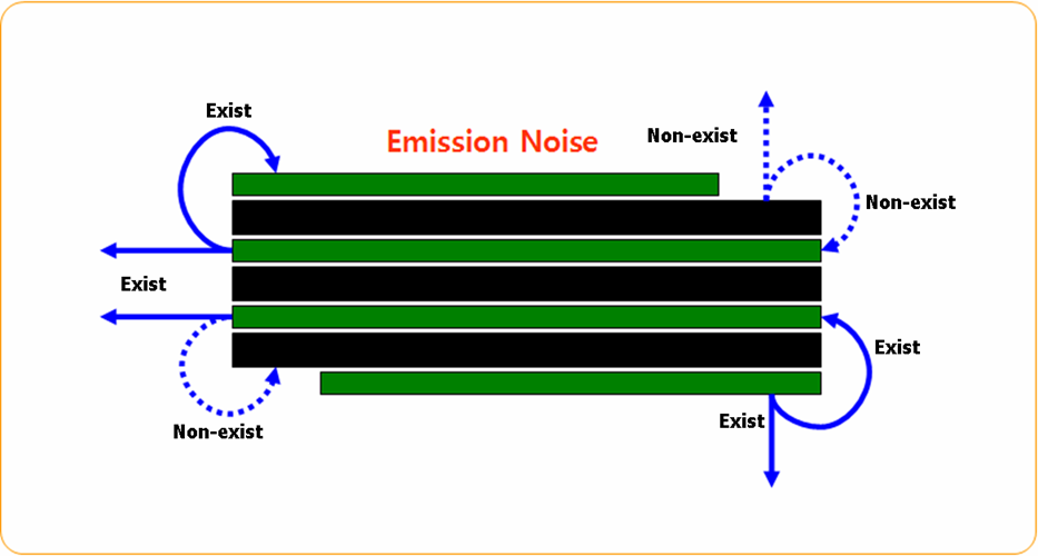
To escape from emission noise from inner layer or outside of PCB, the routing pattern
should have enough clearance from board edges. If the ground or power in inner
layers is too close to board edges, it results in EMI problems on the board.Figure 1.
Rule In Signal Trace Routing
Keep clock signal and high frequency signal trace apart.
Solve EMI/EMC troubles before auto-routing.
Follow the 3-W Rule.
Follow the 20-H Rule.
Figure 2.
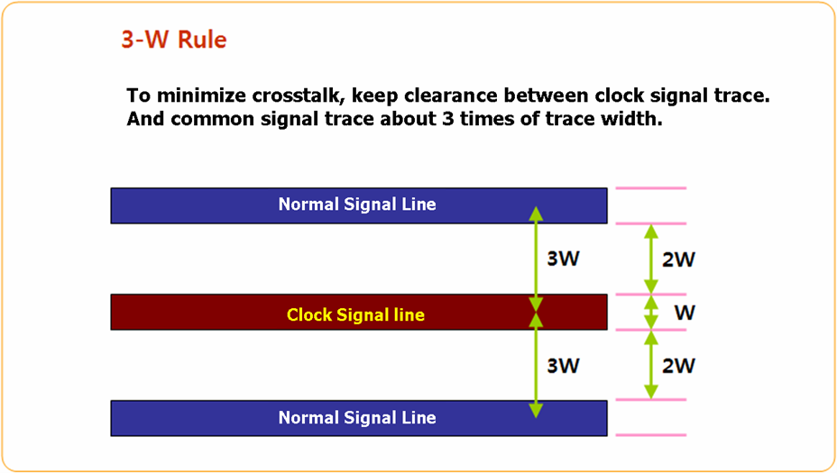
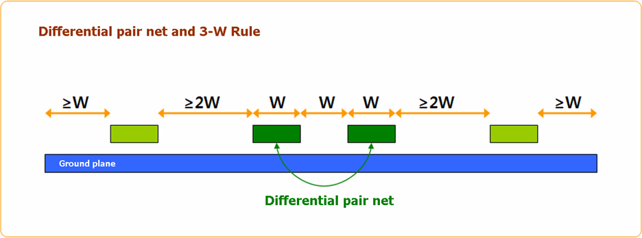
3-W Rule
To minimize crosstalk, keep clearance between clock and signal trace. Common signal
trace about 3 times the trace width.Figure 3. Figure 4.
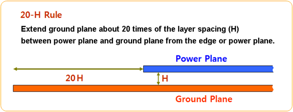
20-H Rule
Extend the ground plane about 20 times of the layer spacing (H) between the power
plane and ground plane from the edge or power plane.Figure 5.