Component
Component to Solder
Checks the clearance between components. A typical example is the clearance checking between the BGA and the chip component.

- Check Layer: Select checking target layer.
- Item: Input item name.
- Comp Group1: Specify the group which will have 3D package shape for its
clearance checking measurement base.
Figure 2. 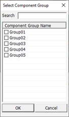
- Measure Base: Select GROUP1’s measurement base defined in the Comp Group1
column.
- Body + Lead: Measurement base will be the dimension of the package body and lead.
- Body: Measurement base will be the dimension of the package body.
- Lead: Measurement base will be the dimension of the package lead.
- Comp Group2: Specify the group which will have pad or solder mask dimension for
its clearance checking measurement base.
Figure 3.
- Measure Base: Select GROUP2’s measurement base defined in Component Group2
column. Some SMD package sizes are smaller than the footprint’s pad dimension.
For these types of components, the measurement base should be considered to Pad
and Solder Mask.
- Pad: Measurement base is pad.
- Solder Mask: Measurement base is solder mask.
- Pad/Solder Mask: Measurement base is the dimension of pad and solder.
- Clearance: Define the clearance distance.
- Ignore Z-Axis: Checks the distance between objects without considering Z-Axis.
BGA Underfill
BGA component is vulnerable to heat stress, shock, and vibration because it has no flexibility. To compensate for these issues, epoxy resin is applied through the underfill process. This item checks whether there is enough space to apply underfill around the BGA components.

- Component Group: Select BGA component that will apply Underfill.
Figure 5.
- Target Layer: Select checking target layer.
- Other Component Clearance
- Reset: Click reset. Recreate the component group list. At this time, existing clearance is also initialized.
- V: PollEx DFA checks for it.
- Group: Specify another component to check BGA component.
- Clearance: Define the clearance between BGA component and another component.
- Underfill: Define the value to apply Underfill.
- Clearance from Component Edge: Define the clearance between the BGA component and the other component to move the Nozzle to apply the Underfill.
- Except Component Group: Define a component group to include as an underfill area. Normally, small chip components placed around the BGA component do not affect the underfill application. Defined in the except component group is recognized as the underfill area.
- Shield-can Comp Group: Specify shield-can group.
- Nozzle Definition: Define nozzle information to apply Underfill.
- Diameter: Enter the diameter of the nozzle.
- Distance from Component Edge: Enter the distance of the nozzle from BGA component.
- Number of Underfill Side: Specify the base of the Underfill area depending on
BGA component size.
- Item: Input item name.
- BGA Size: Enter the size of the BGA component. BGA component size is
based on area.
Figure 6. 
For example, length and breadth width is 5mm ~ 8mm, and then enter 25mm2 ~ 64mm2.
- Number of Side: Specify the number of sides of Underfill area near BGA component.
- Allow for Discontinues Side: Discontinues side of Underfill area.
- Corner: Exclude the corner area of BGA component.
- Remainder: Specify the number of sides of Underfill area for remainder.
- Symmetry: Specify BGA component group to be symmetrical top and bottom/left and right in Underfill area.
- Include Pass Data: In case of verification result, include pass data.
Component Shadow Region
Checks the possible cold solder (spot). A cold spot is an area that does not get sufficient heat to solder because a component is placed next to or between large or high bodied components.

- Remove duplicated results: Remove duplicated results from the lists.
Figure 8. 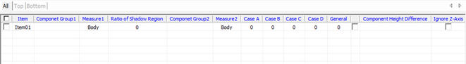
- All/Top/Bottom: Select target layer.
- Item: Input item name.
- Comp Group1: Specify the group which will have 3D package shape for its
clearance checking measurement base.
Figure 9.
- Measure1: Select GROUP1’s measurement base defined in the Item column.
- Body: Measurement base will be the dimension of the package body.
- Lead: Measurement base will be the dimension of the package lead.
- Body + Lead: Measurement base will be the dimension of the package body and lead.
- Body + Pad/Solder Overlap: Measurement base will be the dimension of the package body and pad/solder overlap.
- Pad/Solder Mask Overlap: The measurement is based on the overlapping area between pad and solder mask. It is used when the size of the pad is larger than the component size.
- Ratio of Shadow Region: Define the ratio of shadow region of Comp1 (apply to component body only regardless of measure base).
- Shadow Region Clearance = Height of Comp1 X Ratio of Shadow Region.
Figure 10. 
- Comp Group2: Specify the group which will have 3D package shape for its
clearance checking measurement base.
Figure 11.
- Measure2: Select GROUP1’s measurement base defined in the Measure1 column.
- Body: Measurement base will be the dimension of the package body.
- Lead: Measurement base will be the dimension of the package lead.
- Body + Lead: Measurement base will be the dimension of the package body and lead.
- Body + Pad/Solder Overlap: Measurement base will be the dimension of the package body and pad/solder overlap.
- Pad/Solder Mask Overlap: The measurement is based on the overlapping area between pad and solder mask. It is used when the size of the pad is larger than the component size.
- Case: these are the cases.
Figure 12. 
Figure 13. 
- Component Height Difference: Checks if the difference in height between the two
components is within the set range.
Figure 14.
- Ignore Z-Axis: Checks the distance between objects without considering Z-Axis.