Lines Between Two Pins
Check the number of patterns, the distance between pins, and the distance between pin and patterns.
- Target Layer Definition: Define target checking layer.
- Top/Bottom/All Layers: Select target layer(s) among selections.
- Option
- Check Component placed layer only for DIP type Component: If this option is selected, checking will be done only for DIP type component placed layer.
- Exclude checking for copper polygon shapes: Copper polygon is excluded from verification targets.
- Checking
- Add Component Group into Table: Pressing this button will add new checking lines to the table.
- Check Item: Specify the item name of line.
- Component Group: Specify target components from the component group list.
- APC (Allowable Pattern Count): Give the maximum number of routing patterns between two pins.
- SBP (Spacing between Patterns): Give the clearance value between routing patterns.
- SBPP (Spacing between Pattern and Pad): Give the clearance value between routing pattern and pins.
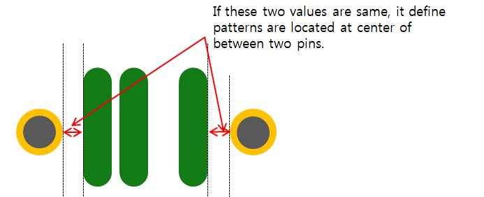
- CL (Center Line): Check whether patterns between two pins are
located in exact center of two pins.
Figure 1. 
- SNE (Same Net Exception): Among patterns, if routing patterns are connected to target pins, they will be excluded in checking.