Bending Area
Check the FPCB bending area.
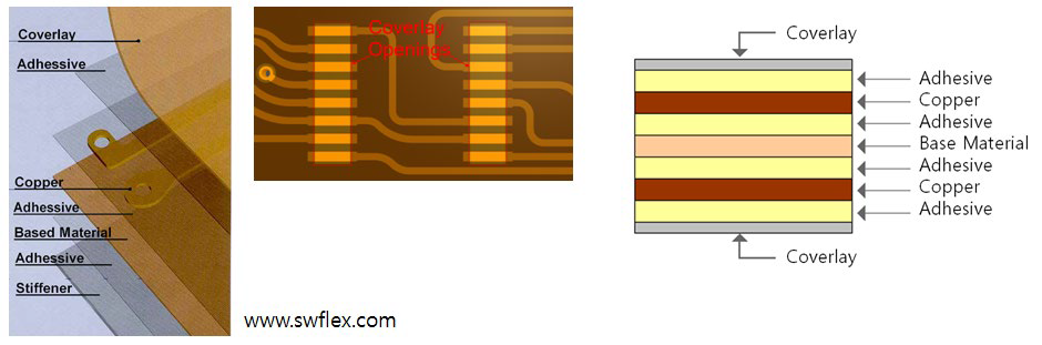
- Coverlay Layer Definition: In FPCB, Coverlay is a flame-retardant
thermosetting epoxy adhesive coated polyimide composite film. Coverlay is
used for protecting and insulating the exposed surface of Flexible Copper
Clad Laminate (FCCL) circuit. Item checks the rule of Coverlay in FPCB.
- Top/Bottom: Select Coverlay layer for top and bottom from layer list.
- Consider Coverlay Data as Negative Representation: If layers for Coverlay are represented as negative type, check this option.
- Checking
- You can define a different checking item for each layer on each line
in the table. In each row, select column and set rule. On a line,
you can define eight different composition rules.
Figure 2. 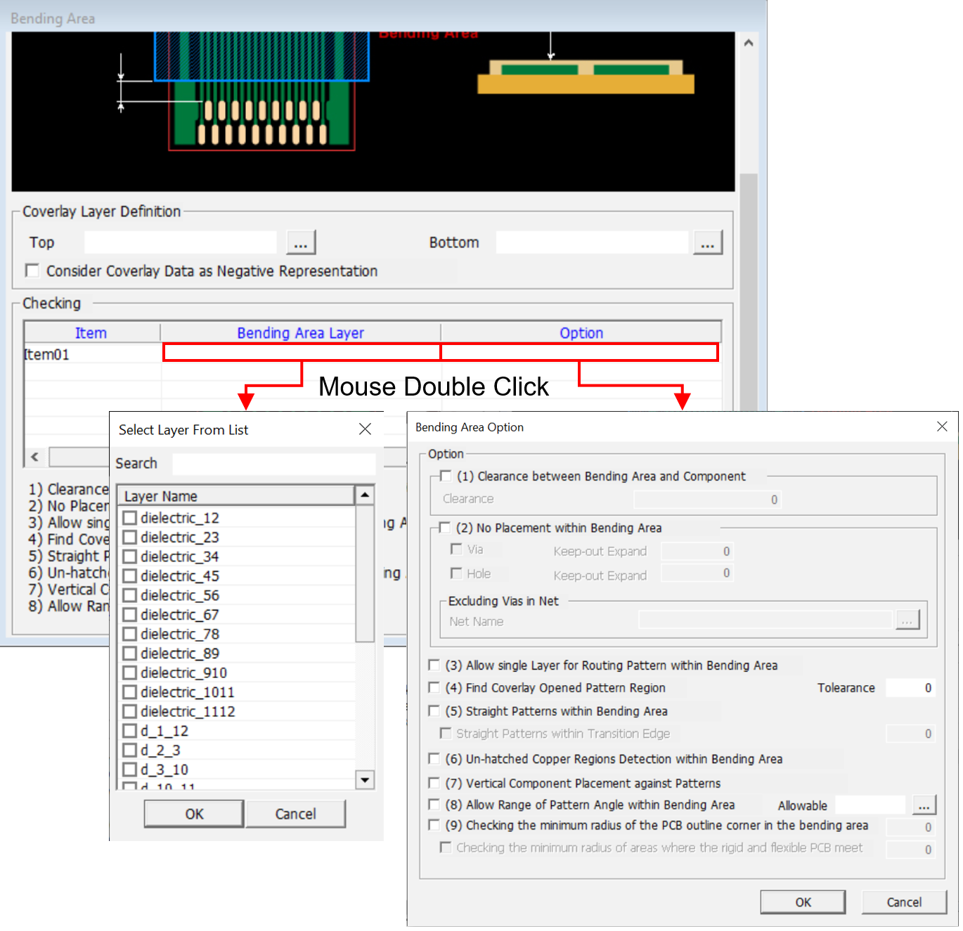
- Item: Specify the item name.
- Bending Area Layer: Select the layer for bending area layer from layer list.
- Option: Upon selecting option column, an option window opens. In the
option window, check and set necessary checking options.
- (1) Clearance between Bending Area and Component: Check the
clearance between bending area and components.
- Clearance: Set the clearance value between FPCB bending area and other components.
- (2) No Placement within Bending Area: Check if vias or holes
are placed in the bending area.
- Via: Check if vias are placed in the bending area.
- Keep-out Expand: To expand the bending area, you can
assign expanding distance.
Figure 3. 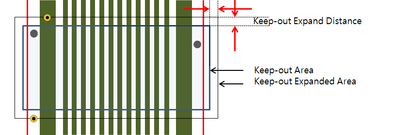
- Hole: Check Holes are placed in the bending area.
- Keep-out Expand: To expand the bending area, you can assign expanding distance.
- Excluding Vias in Net: For vias, connected to certain nets, PollEx DFM will not conduct checking.
- Net Name: Select net names from the net list. For vias connected to selected nets, they will not be checked.
- (3) Allow single Layer for Routing Pattern within Bending
Area: To prevent rigidity, double side routing is not
recommended in the bending area. Checks routing pattern
existence on both sides of the board.
Figure 4. 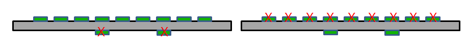
- (4) Find Coverlay opened Pattern Region: If Coverlay is
opened for patterns in the bending area, PollEx DFM finds and defines them as a
fail.
Figure 5. 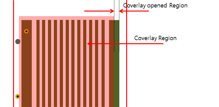
- Tolerance: If the result of Coverlay opened region against pattern is within tolerance, PollEx DFM defines it as passed in checking.
- (5) Straight Patterns within Bending Area: Checks the signal
patterns are all straight in the bending area. If there are
curved regions, PollEx DFM define
them as fails.
- Straight Patterns within Transition Edge: Check patterns are all straight as the user input value from the Rigid PCB Edge.
-
Figure 6. 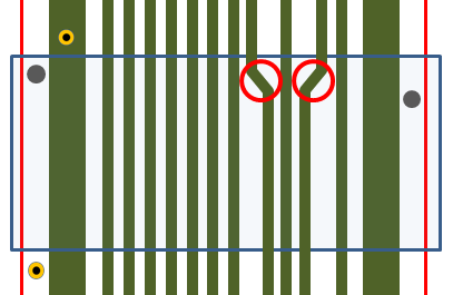
- (6) Un-hatched Copper Regions Detection within Bending Area: If there is a un-hatched copper regions in the bending area, PollEx DFM define them as fails.
- (7) Vertical Component Placement against Patterns: In the
bending area, if there are components placed at the same
direction against the routing pattern, PollEx DFM defines them as fails.
Figure 7. 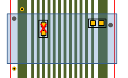
- (8) Allowable Range of Pattern Angle within Bending Area:
Check pattern curved angle is in given ranges.
Figure 8. 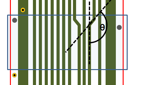
- Allowable: Using floating value input tool, set allowable pattern curved angle ranges.
- (9) Checking the minimum radius of the PCB outline corner in
the bending area: Check if the minimum radius of the PCB
outline corner in the flexible PCB area is designed larger
than the entered value.
- Checking the minimum radius of areas where the rigid and flexible PCB meet: There is a great risk of tearing the FPCB in the area where the rigid PCB and the flexible PCB meet. Therefore, it checks if the minimum Radius of this joint corner is designed to be larger than the entered value.
- (1) Clearance between Bending Area and Component: Check the
clearance between bending area and components.
- You can define a different checking item for each layer on each line
in the table. In each row, select column and set rule. On a line,
you can define eight different composition rules.