Invoke Power Integrity Analysis
To perform PI analysis, you must assign target power net, source pin, load pin, and ground pin.
-
From the menu bar, select .
The Select Power Integrity Analysis Model opens.
Figure 1. 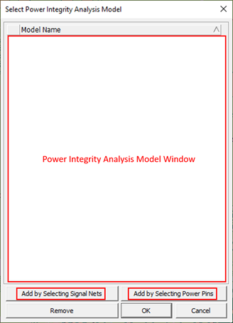
-
Select a power net.
the selected Power Integrity Analysis Model name is displayed in the window. You can remove a model by clicking Remove.
-
Assign the target power net in one of the following ways:
- Select Power Pins: Assign target power net by selecting required power net from power net list. This method is provided for normal PDN and IR-Drop analysis.
- Select Signal Nets: Assign target power net by selecting signal nets. This method is provided for SSN analysis.