Introduction
Power Integrity (PI) ensures that electronic systems receive stable and reliable power by managing the impedance of the Power Delivery Network (PDN), minimizing noise and voltage fluctuations to prevent performance issues and system failures.
As products demand smaller signal swings and more power, Power Integrity (PI) analysis has become crucial. The impedance of the Power Delivery Network (PDN) can cause power issues that make your board's components fail to work correctly. The PI tool helps you analyze and fix these problems.
PollEx PI makes it easy to validate your design choices throughout the entire process, from selecting the board's layer stack-up to placing decoupling capacitors and routing power and ground nets.
PollEx PI is a fast and accurate tool designed for analyzing complex, multi-layer PDNs in PCB designs. Using a high-speed electromagnetic field solver, it helps you find and fix power integrity problems early in the design stage, reducing the need for costly design revisions.
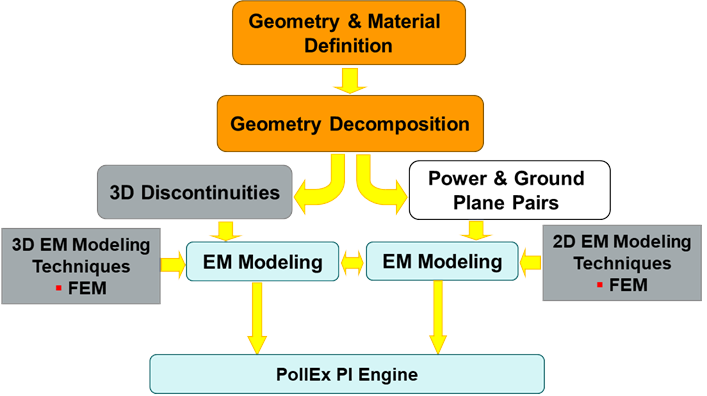
What is PollEx PI
- Analysis of power/ground distribution system performance. Evaluation of
different layer stackup and decoupling capacitor placement:
- Package and PCB model extraction, PDN impedance optimization.
- PCB Core PDN and I/O SSN simulation for noise waveform.
- PCB IR-Drop Analysis.
- Ultra-fast full-wave electromagnetic field solver.
- Advanced pre- and post-layout analysis of power and signal distribution systems.
- Automated, ensures both speed and accuracy:
- Effective utilization of automated meshing technique.
- 3D FEM Full Wave Analysis (Edge effects included).
- Employs structure simplify technique for larger simulation.
- Easy to use interface:
- Direct import Database from all major ECAD tools.
- Implemented as a new design type in the PollEx Design Enclosure and PollEx PCB.
- Shares same modeler interface and similar analysis setup.
- Minimal user training required for existing users of PollEx PCB.
- Major features:
- Handles multi-layer and multi-reference power-ground planes of arbitrary-shape.
- Modular, comprehensive finite element modeling.
- Models for skin effect loss and board/package edge radiated emissions.
- 3D model of via discontinuity.
- Model of split plane discontinuity effects to allow for handling multiple reference planes.
- Interface with comprehensive RLC, SPICE and S-Parameter models for voltage regulator modules.
- Outputs multi-port impedance matrix network for PDN with and/or without decoupling capacitors.
- Accounts for noise couplings between SDN and PDN.
- VIA modeling feature:
- Fast, electromagnetic analysis of signal/power/ground via interactions in multiple-layer boards and packages.
- Supports large number of vias.
- Supports vias with both regular and irregular anti-pads.
- Supports single and differential signaling.
- Outputs single-ended and/or mixed mode S-parameters.
- Supports three types of the edge boundary conditions: Radiation, PMC, and PEC.
- Supports up to twenty+ layer boards.
- Limitation:
- If a via is located on the edge of a plane or the spacing between vias is very narrow, causing anti-pads to overlap, errors may occur in PI analysis.
- The decoupling capacitors are only valid when they are placed on the plane.
- Supports only DC-IR Drop Analysis for composite net.
- Not support the thermal via.
- Not support the via back-drilling.