Edit Properties
-
Edit materials.

-
View PCB's physical stacked information used for power integrity
analysis.
-
From the menu bar, select .
The Layer Stacks window shows PCB's stacked information.
The stacking order, thickness, and material properties of metallic and dielectric layers are critical factors that greatly affect signal transmission and thermal distribution in PCB designs.
It's important to accurately define the Layer Type, Thickness, and Conductor/Dielectric Materials to ensure optimal performance. Always verify that the total thickness is within acceptable limits for your design.

-
From the menu bar, select .
-
View part property assignment.
-
From the menu bar, select .
- The Parts dialog shows the status of the properties assignment to the parts which are included in the current PCB system to analyze. Functional Type and Cost of each component are editable from this dialog.
- The Parts dialog shows also the Model Type, Model File and Model Name if there is part assigning with SPICE or S-Parameter model.
Figure 1. 
-
From the menu bar, select .
-
From the menu bar, select to view pad-stack information used in the design.
You cannot modify the parameters from this dialog.

-
Select to view selected signal net information.
You cannot modify the information from this dialog.
-
Select to view target power and ground net information.
You cannot modify the information from this dialog.

-
Select to view receiver component information.
You can edit the Placed Layer from this dialog.
Figure 2. 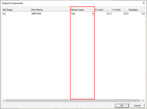
-
Select to view power source component information.
You can edit the Placed Layer and also RLC values from this dialog.
Figure 3. 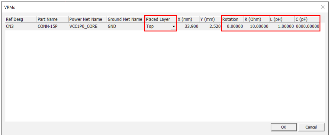
-
Select to view power load component information.
You can :
- choose each port you want to use on this dialog
- edit the DC Current (mA) for DC IR-Drop analysis from this dialog
- edit the R (ohm), L(nH) and C(pF) value for each ports
Figure 4. 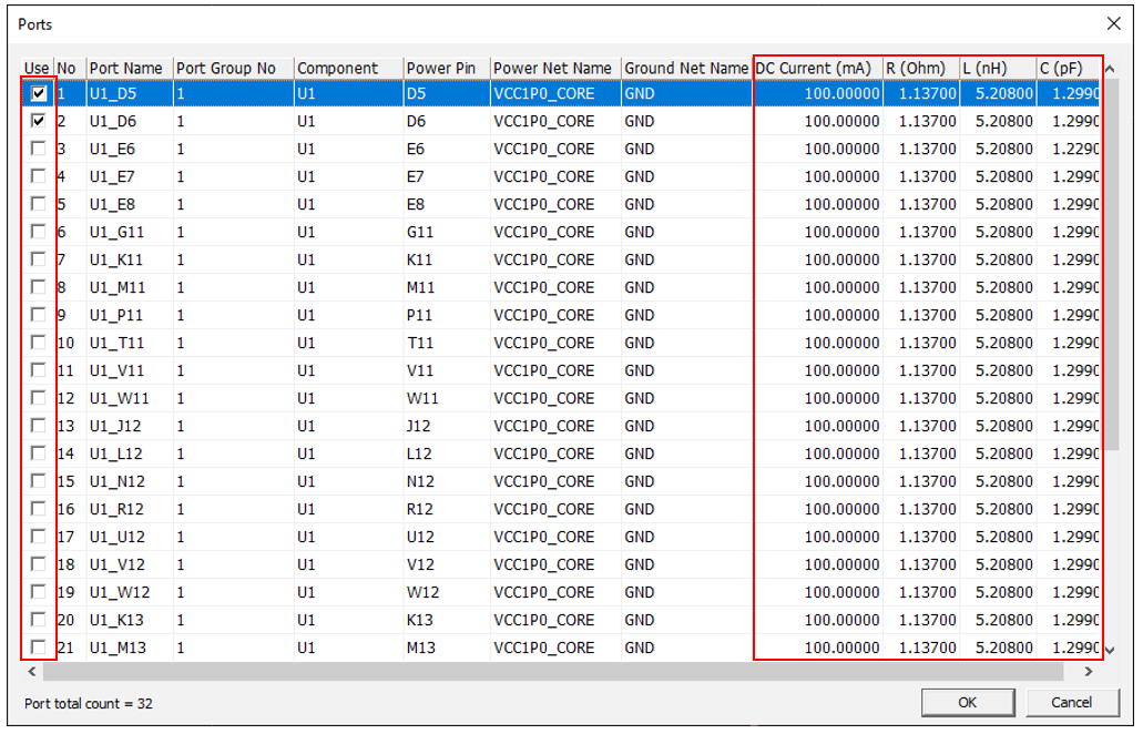
-
Select to view current test case and capacitor information.
- Add Case: Add the new test case. The test case applies only to PDN analysis.
- Copy Case: Add the new test case while maintaining the capacitor information of selected test case.
- Remove Case: Remove selected test case.
- Assign Decaps: Assign a value to the selected capacitor. Upon clicking this menu, the Assign Decaps dialog opens. By clicking required capacitor, the capacitor value will be changed.
- Show Decap Location Property: Open the Decap Location Property dialog
which displays whole capacitor information.

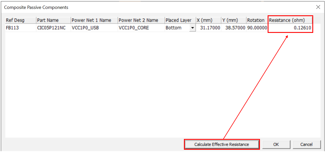
-
Select to view composite passive components connected to the selected
power net (Exclude Capacitors).
You can calculate Effective Resistance if there is composite passive component which is importing S-parameter data from this dialog.
Figure 5.