PollEx DFE+ is one of many PollEx tool
sets and it checks electrical validity of PCB design. It is a combination of a rule
check tool and an analysis tool. The DFE+ uses the SI, PI, and thermal analysis
engine to examine the result of the analysis to see if it meets the target
electrical value.
PollEx DFE+ can be launched within PollEx PCB, and by testing with the result of the analysis
rather than the geometry value, PollEx DFE+ helps you to
reduce cost and time to produce good working PCBs fast.
The PollEx DFE+ results can be outputted to a well-formatted
MS/Excel spreadsheet.
This tutorial is primarily designed to enable you to get a quick start with the
PollEx DFE+ tool. It is not intended to be a complete
reference guide for all the available test items but will give you an overview of
key concepts. Understanding these concepts will allow you to learn how to use this
tool efficiently with the help of the online documentation. Press
F1 to access the online help
from within the software.
This tutorial shows simple design check flow using PollEx DFE+ with a fairly simple design. Studying this example carefully will help you become
familiar with the PollEx DFE+ tool.
After downloading the file, unzip it and save the file into a folder. That file
saving folder is the job folder in this tutorial.
Create Project
From the menu bar, click File > Open and open the
PollEx_PCB_Sample_r<revision_number>.pdbb
file from
C:\ProgramData\altair\PollEx\<version>\Examples\PollEx_PCB_Sample_r<revision_number>.pdbb.
From the menu bar, click File > Save As Project.
The Save As Project dialog displays.
Enter a new project name and select the Project folder to put in the design
folder.
Click OK to close this dialog
to use the default name.
You can change the project name and the project folder name to put in the
design folder. The project directory is created under the design folder, and
PollEx_PCB_Sample_r<revision_number>.pdbb
and related files are copied into the project directory. The current directory
is automatically changed to the project directory.
Preview PCB Design.
The sample design consists of CPU and two DDR3 memories.
Build PCB Stack
From the menu bar, click Properties > Layer Stack.
The Layer Stack Manager dialog opens.
Click Import.
The Explorer dialog opens.
Find the directory path of your own stack-up files in the navigation tree
section.
You will use the training.udls file from
C:\ProgramData\altair\PollEx\<version>\Examples\Verification\DFEP\Stackup.
PollEx also provides a default stack-up, the path is:
Install Directory\Data\Layer.
Select training.udls for this 6-layer stack-up.
Click OPEN to load and close the
Explorer dialog.
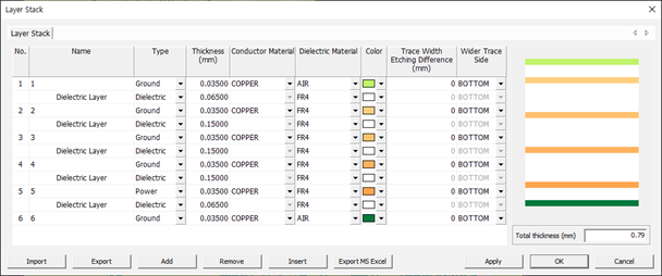
Your stack-up should now look as follows: Figure 1.
Click OK to close the
Layer Stack Manager dialog.
Assign IBIS Model to DDR3 Memory Device
From the menu bar, click Properties > Parts.
The Parts dialog opens.
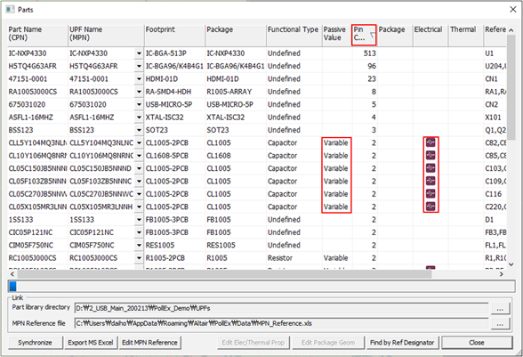
Sort the result by double-clicking Pin Count.
The passive component RLC values are automatically extracted from PDBB data,
if the value property was correctly assigned in the PDBB database. The passive
value types of the passive component are classified into variable and fixed.
Fixed: Use the passive value defined in UPE. You cannot change the
value.
Variable: You can assign the passive component value using the
Properties-Components menu.
Figure 2.
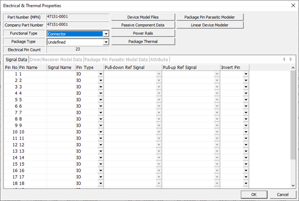
Assign Electrical Simulation Model.
Double-click the part H5TQ4G63AFR.
The Electrical & Thermal Properties
dialog opens.
Click Device Model Files.
The Device Model Files dialog
opens.
Click Add in the Device Model
Files dialog.
The Model File dialog opens.
Click to
search and select the Memory.ibs file from
C:\ProgramData\altair\PollEx\<version>\Examples\Verification\DFEP\Simulation_Model
for DDR3 Memory device.
Click Open.
Click OK to close the
Model Files dialog.
The Device Model Files dialog
opens.
To close the Device Model Files dialog, click
OK.
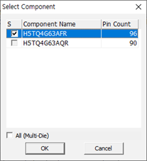
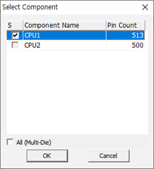
When the IBIS file contains numbers of different components (IC
devices), you need to select one of them. Pin count can be a good
reference to select the right one. The Select
Component dialog displays.
Select the first component, and click OK to close the Select
Component Manager dialog.
Figure 3.
The Electrical & Thermal Properties
dialog opens.
Setup Power Information.
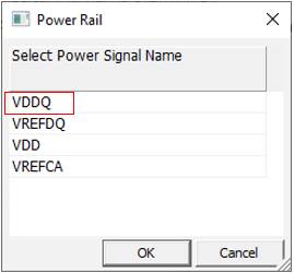
Click Power Rails.
The Power Rail dialog displays. All the
power rails used for this component are displayed in the middle of this
dialog.
Click the VDDQ power rail.
Figure 4.
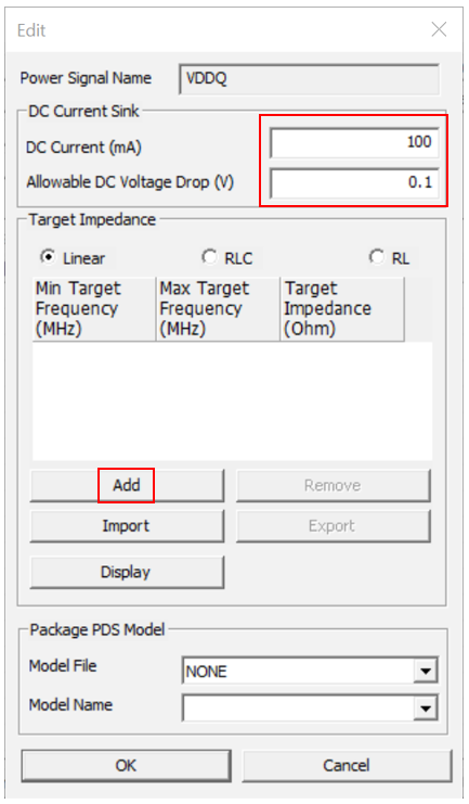
The Edit dialog opens.
Enter 100 for the DC Current.
Enter 0.1 for the Allowable DC Voltage
Drop.
Your settings should now look as follows: Figure 5.
Click Add to setup Target Impedance.
The first row of the target impedance field is
added.
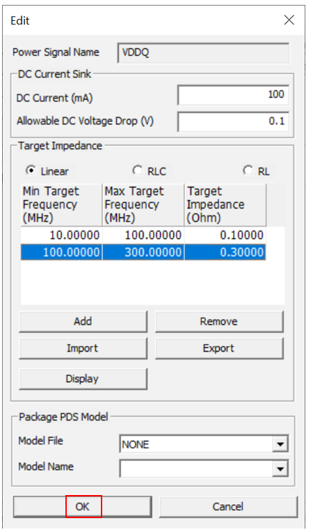
Enter 10 for the Min Target Frequency.
Enter 100 for the Max Target Frequency.
Enter 0.1 for the Target Impedance.
Click Add.
The second row of the target impedance field is
added.
Enter 100 for the Min Target Frequency.
Enter 300 for the Max Target Frequency.
Enter 0.3 for the Target Impedance.
Your settings should now look as follows: Figure 6.
Click OK to close the
Edit dialog.
Click the VREFDQ power rail.
The remaining steps are the same as the steps above.
Click the VDD power rail.
The remaining steps are the same as the steps above.
Click the VREFCA power rail.
The remaining steps are the same as the steps above.
Click OK to close the
Power Rail dialog.
Click OK to close the
Electrical & Thermal Properties
dialog.
The Electrical icon of the H5TQ4G63AFR device
appears.
In this step, you will assign function type to power component.
To perform PI analysis, you should assign the power source
component. If the Function Type is Connector or Power for a component, the PollEx PI considers this component as the power source.
Double-click the part 47151-0001 in the dialog invoked
by clicking Properties > Parts.
The Electrical & Thermal Properties dialog
opens.
Select Connector for the Functional Type.
Figure 8.
Click OK to close the
Electrical & Thermal Properties dialog.
Double-click the part 675031020 in the dialog.
Select Connector for the Function Type.
Assign Passive Component Data to R and C
Double-click the part RC1005J101CS in the
Parts dialog.
The Electrical & Thermal Properties dialog
displays.
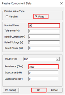
Click Passive Component Data in the Electrical
& Thermal Properties dialog.
The Passive Component Data dialog
opens.
For Passive Value Type, select Fixed.
Enter 1K for Nominal Value.
Enter 1000 for the Resistance (ohm).
Figure 9.
Click OK to close the
Passive Component Data dialog.
Click OK to close the
Electrical & Thermal Properties dialog.
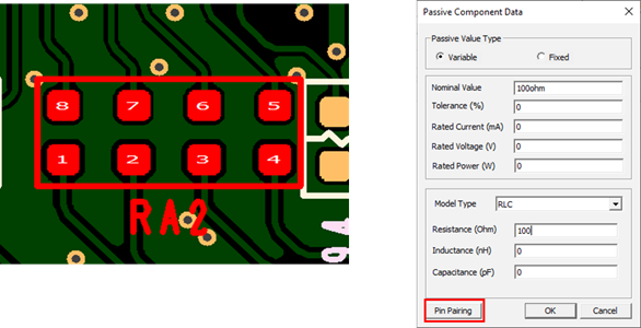
Assign Passive Component Data to Array R and C
When a passive is an array component, you need to define the pin pair
configuration. Figure 10.
Double-click the RA1005J000CS part that has more than
two pins in the Parts Dialog.
Click for the Functional Type and select Resistor.
Click Passive Component Data in the Electrical
& Thermal Properties dialog.
For Passive Value Type, select Fixed.
Enter 100 ohm for the Resistance.
Figure 11.
Click Pin Pairing in the Passive Component
Data dialog to open the Pin Pairing
dialog.
Click Add to define pin pairs.
The specified passive component values are assigned separately to these paired
pins. Figure 12.
Close any opened dialogs.
Assign Part Property from UPE
In this step, you will import all required PART properties from Unified Part Editor
(UPE).
The unified parts created by PollEx UPE can have versatile
information, such as electrical buffer model, package thermal parameters, and 3D
package geometry, which is needed for electrical, thermal, and 2D/3D assembly
analysis (by PollEx DFA and PCB assembly viewer). It is
stored in specific folders in local or server systems.
Link the unified parts.
From the menu bar, click Properties > Parts.
The Parts Manager dialog
opens.
Click in the Part library directory menu.
To explore the library path for the unified parts, select the Part
folder and then click OK.
UPF path: C:\<working directory>\Part
Click Synchronize to start assigning the part
properties.
Figure 13.
Content names under the UPF Name column denotes that the UPF file
exists under the local Parts folder for those parts.
The icon under the Package column denotes that 3D package
geometry is linked with the unified part.
The icon under the Electrical column denotes that the
electrical buffer model is called from the unified
part.
The icon under the Thermal column denotes that thermal
information is called from the unified parts.
Click Close to close the
Parts dialog.
Add New Class Item
From the menu bar, click Properties > Net Classes.
The Net Classes dialog opens.
Click Add.
The ADD dialog opens.
Enter the net class name SDA_BUS in the net Class Name
field and type search string *SDA*# in the Search Strings
field.
Click Add String.
Click OK to close the
ADD dialog.
The SDA_BUS net class is registered in the Net
Classes dialog. Figure 14.
Click OK to close the
Net Classes dialog.
From the menu bar, click Properties > Nets.
The Nets dialog opens.
Click Find Net Class to assign net class using the
pre-defined net class file.
Three nets are classified as SDA_BUS net class.
Assign Net Properties for Power
From the menu bar, click Properties > Nets.
The Nets dialog displays.
Double-click VCC1P5_DDR.
The Edit dialog displays.
Select the Net Type as Power, enter
1.5 for the Voltage, and click OK.
Figure 15.
Double-click 5VCC.
Select Power for the Net Type, enter
5.0 for the Voltage, and click OK.
Double-click DCDC_5V.
Select Power for the Net Type, enter
5.0 for the Voltage, and click OK.
Double-click SCL_5V.
Select Power for the Net Type, enter
5.0 for the Voltage, and click OK.
Double-click SDA_5V.
Select Power as the Net Type, enter
5.0 for the Voltage, and click OK.
Double-click VCC2P8_GMAC.
Select Power as the Net Type, enter
2.8 for the Voltage, and click OK.
Assign Net Properties for Differential Pair
Double-click MCU_ACK.
The Edit dialog displays.
Change the Net Type to Diff Signal +.
Select the other pair net MCU_ACKB as Diff Signal using
the scroll bar.
Figure 16.
Click OK to close the
Edit dialog.
You will find that the MCU_ACK net and MCU_ACKB net are combined as a
differential pair net. Figure 17.
Click OK to close the
Nets dialog.
Assign Net Properties Automatically
From the menu bar, click Properties > Nets.
The Nets dialog displays.
Click Assign Net Type.
The PollEx DFE+ sets the properties for all
nets automatically using net information described in IBIS files and
property. Figure 18.
Click OK to close the
Nets dialog.
Create Composite Net
From the menu bar, click Properties > Composite Nets.
Activate the Resistor and
Capacitor checkboxes.
Click Generate Composite Net.
You can specify nets that should not be composited with other nets such as
Power and Ground nets.
The Selects Nets to Exclude dialog
opens.
Click OK and check the listed
composited nets.
Figure 19.
If you click Composite Data or Pin
List, you can review composite net structure or pin list. If you
want to check the total net composition status for the composited nets, use the Tools > Net 2D/3D Viewer menu. Figure 20.
Select the composite net
CN-||MCU_HDMI_HPD||NetCN1_19||.
The secondly listed composited net above configured with MCU_HDMI_HPD and
NetCN1_19 displays at the beginning of this composite net chapter having R85
resistor. Figure 21.
Close the Net 2D/3D Viewer dialog.
Create HDMI Bus Group
From the menu bar, click Properties > Net Buses/Groups.
The Net Buses/Groups dialog opens.
Click Generate DDR Buses.
The DDR Bus groups is automatically generated.
Click Add to generate a new bus group.
The Add Net Bus/Group dialog opens.
Enter HDMI_BUS in the Net bus/group name field.
Enter 10 in the Max allowable bus skew(ps) field.
Enter 10 in the Max allowable strobed skew(ps)
field.
Click Selected Strobe Net to select strobe net.
The Net List dialog opens.
Select the CN-||MCU_HDMI_TXC_N|| and
CN-||MCU_HDMI_TXC_P|| nets as a strobe net.
Click OK to close this
dialog.
Figure 22.
Click in the Control device region and select U1 as a
driving component of this bus.
Click Select Net to select belonging net.
The Net List dialog opens.
Select the other HDMI nets except the clock net as the belonging nets.
Click OK to close this
dialog.
Click OK to close this
dialog.
The HDMI_BUS group is registered as a new bus group with the name
HDMI_BUS.
Define Component Group
From the menu bar, click Option > DFE+ > Input to launch PollEx DFE+.
The PollEx DFE+ Design Constraints dialog
opens.
Define CPU component group.
In the Component Group Type section, click Component
Group01 and change the group name to CPU by
double-clicking the Name column.
In the Type section, select PART from the
drop-down menu.
Click the CPU component group that was created
and select Select Components from List from the
context menu.
Figure 23.
The Select Components from List dialog
opens.
Select the IC-NXP4330 component from the part
name list in lower section.
Click Add to add selected component to selected
item.
Figure 24.
Click OK.
Define Passive component group.
In the Component Group Type section, click Component
Group02 and change the group name to
Passive by double-clicking the
Name column.
In the Type section, select Reference from the
drop-down menu.
Click the Passive component group that was
created and select Select Component from List
from the context menu.
The Select Components from List dialog
opens. This menu will show you the reference name list.
Enter R in the search field, select the
Resistor component, and click
ADD.
The highlighted items will be moved to Reference name field. Figure 25.
Enter C in the search field, select the
Capacitor component, and click
ADD.
In the Reference Name field, select CN1 and
CN2 and click
Remove.
Figure 26.
Enter FB in the search field, select the
Inductor or bead
component, and click ADD.
The highlighted items are moved to the Reference name
field.
Enter TP in the search field, select the
test-point component, and click
ADD.
The highlighted items are moved to Reference name
field.
Click OK to close
Select Component From List dialog.
Define Net Group
Define Single-Ended net group.
In the Net Group section, double-click Net
Group01 and change the group name to
Single_Ended by double-clicking the
Name column.
In the Type section, select Net from the
drop-down menu.
Click the Single_Ended net group that was
created and select Select Nets From List from the
context menu.
Figure 27.
The Select Net from List dialog opens.
Select the MCU_AA0 and
MCU_AA1 nets from the signal net list.
After net selection, click Add to List to add
the selected net list to the selected item.
Figure 28.
Click Done to close this window.
Define DDR_Address net group.
In the Net Group section, double-click Net
Group02 and change the group name to
DDR_Address by double-clicking the
Name column.
Click the DDR_Address net group that was created
and select Select Net List from the context menu.
The Select Net from List dialog
opens.
Select the MCU_AA10 and
MCU_AA11 nets from the signal net list.
Click Add to List to add the selected net list
to the selected item.
Click Done to close this window.
Define DDR_CLK net group.
In the Net Group section, double-click Net
Group03, and change the group name to
DDR_CLK by double-clicking the
Name column.
Click the DDR_CLK net group that was created and
select Select Net From List from the context menu.
The Select Net from List dialog
opens.
Select the MCU_ACK and
MCU_ACKB nets from the signal net list.
Click Add to List to add the selected net list
to the selected item.
Click Done to close this window.
In the Net Group section, your net group setting should now look as
follows.Figure 29.
Define DDR_Byte0 net group.
In the Net Group section, double-click Net
Group04, and change the group name to
DDR_Byte0 by double-clicking the
Name column.
Click the DDR_Byte0 net group that was created
and select Select Net From List from the context menu.
The Select Net from List dialog
opens.
Select MCU_D0 ~ MCU_D7 from signal net
list.
Click Add to List to add the selected net list
to the selected item.
Click Done to close this window.
In the Net Group section, your net group setting should now look as
follows:Figure 30.
Define DDR_DQS net group.
In the Net Group section, double-click Net
Group05, and change the group name to
DDR_DQS by double-clicking the
Name column.
Select the DDR_DQS net group that was created
and select Select Net From List from the context menu.
The Select Net from List dialog
opens.
Select the MCU_NADQS0 and
MCU_PADQS0 nets from the signal net
list.
Click Add to List to add the selected net list
to the selected item.
Click Done to close this window.
In the Net Group section, your net group setting should now look as
follows:Figure 31.
Define Differential net group.
To add a line to the Net Group table, enter 1 in
the Group No. field, and click Add Groups.
An additional line is added in the Net Group table.
In the Net Group section, double-click the newly added line, and change
the group name to Differential by double-clicking
the Name column.
Click the Differential net group that was created and select
Select Net From List from the context menu.
The Select Net from List dialog
opens.
Select the MCU_HOST_USB- and
MCU_HOST_USB+ nets from the signal net
list.
Click Add to List to add the selected net list
to the selected item.
Click Done to close this window.
In the Net Group section, your net group setting should now look as
follows:Figure 32.
Check Impedance
Enable the Impedance checkbox.
The PollEx-DFE+ Design Constraints dialog
opens.Figure 33.
Set Impedance test condition.
Double-click the Net Group field of the first
item.
The Select Object Group dialog box
opens.
Select the Single_Ended net group and click
OK.
Figure 34.
Double-click the Target Impedance field of the
first item.
The Target Impedance dialog
opens.
Enter 50 for Main.
Enter 60 in the Break In.
Enter 10 in the
Tolerance
of Main.
Click OK.
Figure 35.
Double-click the Option field of first
item.
The Option dialog opens.
For Plane Option, select Real.
Figure 36.
Click OK to close
this dialog.
With this setting, PollEx DFE+ will check if
the impedance of MCU_AA0 and MCU_AA1 signal is within target impedance
range.
Define differential net impedance check condition.
Double-click the Net Group field of the second
item.
The Select Object Group dialog
opens.
Select the Differential net group and click
OK.
Figure 37.
Double-click the Target Impedance field of the
first item.
The Target Impedance dialog box
opens.
Setup Characteristic impedance of differential line.
Enter 50 for Main.
Enter 60 for Break In.
Enter 10 for Tolerance of Main.
Setup Differential impedance of differential line.
Enter 90 for Main.
Enter 100 for Break In.
Enter 15 for Tolerance of Main.
Click OK.
Figure 38.
Double-click the Option field of the first
item.
The Option dialog opens.
For Plane Option, select Real.
Figure 39.
Click OK.
With this setting, PollEx DFE+ will check if
the differential impedance of MCU_HOST_USB- and MCU_HOST_USB+
differential pair is within target impedance range.
Run Impedance Item and review Check Result.
Click Save As and save the input file as
training.DFEPI in the PollEx
DFEP folder under the job folder.
You can reload this input setup condition by clicking
Load.
Click Start Checking.
PollEx DFE+ starts checking for
selected checking items. PollEx DFE+ changes
the window for results display.
In the Result tab, select [Signal Integrity]
Impedance and choose the first error checking
item.
Figure 40.
By reviewing the image window on the right, we can see that this
kind of error can’t be fixed by modifying the design. This kind of error
can be excluded from the error list by using check option.
In the result tab window, click View
Input.
The PollEx DFE+ Design Constraints dialog
opens.
In the Check Item Category section, click the
Impedance item to set the test
condition.
The Impedance item rule entry dialog
opens.
Double-click the Options field of the first
item.
The Option dialog opens.
Enable the Pin Escape checkbox and enter
0.5 in the value field.
Enable the Via Escape checkbox and enter
0.5 in the value field.
Figure 41.
Click OK to close
Option dialog.
Click Start Checking.
PollEx DFE+ prompts you to save current input
file status or not.
Click Save.
PollEx DFE+ starts checking with new input
condition.
In the result tab, select Impedance and review
the result item.
The previous 1st case error is removed.
Select other checked items and review the results.
Check Timing Skew
Preview Timing Skew item.
In the result tab window, click View Input.
The PollEx DFE+ Design Constraints dialog
opens.
Enable the Timing Skew checkbox in the Check Item
Category list.
The Timing Skew Item Rule Entry dialog
opens.
Strobed BUS Skew check setup.
In the Timing Skew Input Setup dialog, click the Check
Type field of Item01 and select Strobed BUS
Skew.
In the Timing Skew Input Setup dialog, click the
Net Group field to select the target net from
the net group list.
The Select Object Group dialog
opens.
Select the DDR_Address net group as a target net
group and click OK.
Select Strobe Net.
In the Timing Skew Input Setup dialog, click the
Strobe Net field to select a strobe net from
net group list.
The Select Object Group dialog
opens.
Select the DDR_CLK net group as a strobe net
group and click OK.
Click the Start Component field in the
Timing Skew Input Setup dialog to select a
Start Component from the component group list.
The Select Object Group dialog
opens.
Select the CPU component group as the start
component group and click OK.
Click the Except Component field in the
Timing Skew Input Setup dialog to select the
Passive component Group from the component group list.
The Select Object Group dialog
opens.
Select the Passive component group as an exclude
component group and click OK to close this dialog.
Click the Period(ns) field in the
Timing Skew Input Setup dialog and enter
2.
Click the Skew(pS) field in the Timing
Skew Input Setup dialog and enter
0.1.
The allowable skew between BUS nets and strobe net is within
0.1ps.
Select Tolerance(%).
Click the Tolerance(%) field in the
Timing Skew Input Setup dialog and enter
10.
Click the Analyze Option field in the
Timing Skew Input Setup dialog to setup
simulation environment.
The Timing Skew dialog opens. You can
change the actual driver pin model among selectable models. Figure 42.
Select Use user defined buffer model.
If you check Use pre-defined buffer model,
default Driver and Receiver models from UPE will be used.
In the Model field for Strobe Net, click and select
PBLPDDR3_DQS_60ohm.
In the Model field for Net, click and select
PBLPDDR3_60ohm.
In the Model field for Receiver Strobe Net, click and select
clk.
In the Model field for Receiver Net, click and select
input.
Click OK to close
Timing Skew dialog.
BUS Skew check setup.
Click the Check Type field of Item02 in the
Timing Skew Input Setup dialog and select
BUS Skew.
Click the Net Group field to select a target net
from net group list.
The Select Object Group dialog
opens.
Select the DDR_Address net group as a target net
group and OK.
Click the Start Component field in the
Timing Skew Input Setup dialog to select a
Start Component from the component group
list.
The Select Object Group dialog
opens.
Select the CPU component group as the start
component group and click OK.
Click the Except Component field in
Timing Skew Input Setup dialog and select the
Exclude Component from component group
list.
The Select Object Group dialog
opens.
Select the Passive component group as a exclude
component group and click OK.
Click the Period(ns) field in the
Timing Skew Input Setup dialog and enter
2.
Click the Skew(ps) field and enter
0.1.
Allowable skew between BUS nets and strobe net is within 0.1ps.
Click Tolerance(%).
Click the Tolerance(%) field in Timing
Skew Input Setup dialog and enter
10.
Click the Analyze Option field to setup the
simulation environment.
The Timing Skew dialog opens. You can
change the actual driver pin model among selectable models. Figure 43.
Select Use user defined buffer model.
If you check the Use pre-defined buffer model, default Driver and
Receiver models from UPE will be used.
In the Model field for Driver Net, click and select
LBLPDDR3_60ohm.
In the Model field for Receiver Net, click and select
input.
Click OK to close the
Timing Skew dialog.
Differential Skew check setup.
Click the Check Type field of Item03 in the
Timing Skew Input Setup dialog and select
Differential Skew.
Click the Net Group field to select a target net
from the net group list.
The Select Object Group dialog
opens.
Select the DDR_CLK net group as a target net
group and click OK.
Click the Start Component field in the
Timing Skew Input Setup dialog to select a
Start Component from the component group
list.
The Select Object Group dialog
opens.
Select the CPU component group as a start
component group and click OK.
Click the Except Component field in the
Timing Skew Input Setup dialog to select a
Exclude Component from component group
list.
The Select Object Group dialog
opens.
Select the Passive component group as a exclude
component group and click OK.
Click the Period(ns) field in the
Timing Skew Input Setup dialog and enter
2.
Click the Skew(ps) field and enter
0.1.
Allowable skew between BUS nets and strobe net is within 0.1ps.
Click Tolerance(%).
Click the Tolerance(%) field in the
Timing Skew Input Setup dialog and enter
10.
Click the Analyze Option field to setup a
simulation environment.
The Timing Skew dialog opens. Figure 44.
Click Use pre-defined buffer model.
The default Driver and Receiver models from UPE will be used.
Click OK to close
Timing Skew dialog.
Check Timing Skew.
Disable the Impedance checkbox in the Check Item
Category section.
Enable the Timing Skew checkbox in the Check
Item Category section.
Figure 45.
Click Start Checking.
Click Save to save the current setup.
PollEx DFE+ starts checking for selected
checking items. After running, PollEx DFE+
changes the window for results display.
In the result tab, click the [Signal Integrity] Signal
Integrity item to see the detailed result.
Figure 46.
Review the Timing Skew Check Result.
In the result tab, select [Signal Integrity] Timing
Skew to see the detail result.
Figure 47.
In the left side of the window, you can see the error status. The
strobed timing skew between MCU_AA10 and MCU_ACK strobe signal is bigger
than our limit 0.1ps, so it fails. (The exact result values may vary
slightly depending on the solver update.)
Choose the first error checking item of this section.
The MCU_AA10and MCU_ACK nets are highlighted in right side
window. The Waveform Viewer dialog
opens.
Click Close.
Select the first error item and click
Analyze.
The Network Analysis dialog opens. You can
modify the simulation parameter or change the topology to resolve this
problem. Refer to the SI or
SI Tutorial for more
details.
Click Close.
Check Crosstalk Noise
In the result tab window, click View Input.
The PollEx DFE+ Design Constraints dialog
opens.
Enable the Crosstalk Noise checkbox in the Check Item
Category list.
Set Crosstalk Noise check condition.
Click the Net Group field in the
Crosstalk Noise Input Setup dialog to select a
target net from net group list.
The Select Object Group dialog
opens.
Select the DDR_Address net group as a target net
group and click OK.
Click FEXT(mV).
Click the FEXT(mV) field in the
Crosstalk Noise Input Setup dialog and enter
10.
Click NEXT(mV).
Click the NEXT(mV) field and enter
10.
Click the Analyze Option field to setup a
simulation environment.
The Display Coupling dialog
opens.
Select Use pre-defined buffer model.
The default Driver and Receiver models from UPE will be used.
Click OK to close the
Display Coupling dialog.
Figure 48.
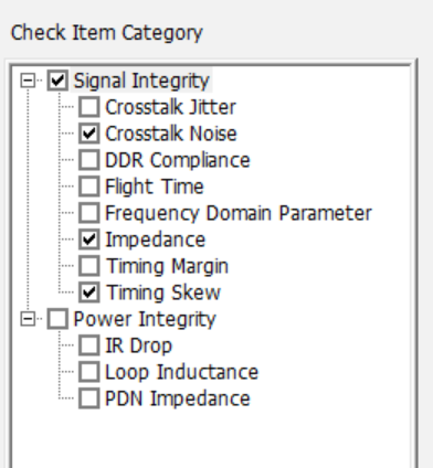
Check Crosstalk Noise item.
Disable the Impedance and Timing
Skew checkboxes in the Check Item Category
section.
Enable the Crosstalk Noise checkbox.
Figure 49.
Click Start Checking.
Click Save to save current setup.
PollEx DFE+ starts checking for
selected checking items. After running, PollEx DFE+ changes the window to results
display.
In the result tab, click [Signal Integrity] Crosstalk
Noise to see the detailed result.
Figure 50.
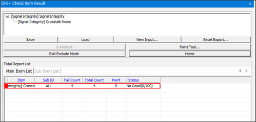
Review the Crosstalk Noise Check Result.
In the result tab, select [Signal Integrity] Crosstalk
Noise to see the detail result.
In the left side of the window, you can see the error status. The
amount of near-end crosstalk noise for the victim net MCU_AA10 is bigger
than the 10mV limit, so it fails. (The exact result values may vary
slightly depending on the solver update.)
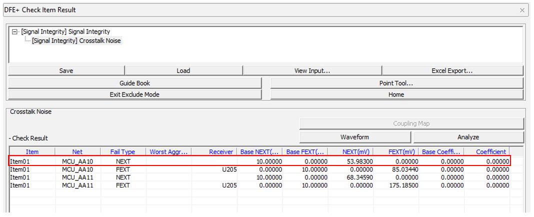
Click the first error checking item of this section.
The victim net MCU_AA10 net is highlighted in right side window.
The Waveform Viewer dialog opens.
Click Close.
Select the first error item and click
Analyze.
The Crosstalk Analysis dialog opens. You
can modify simulation parameters, topology, or driver strength to
resolve this problem. Refer to SI or SI Tutorial for more details.
Click Close.
Create Excel Report for Result
In the result tab, click View Input.
The PollEx DFE+ Design Constraints dialog
opens.
Enable the Impedance, Timing
Skew, and Crosstalk Noise checkboxes.
Figure 51.
Click Start Checking.
Click Save.
PollEx DFE+ starts checking for selected
checking items. After running, PollEx DFE+ changes the
window for results display.
Click Save.
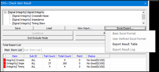
We can read this result file using the Option > DFE+ > Result menu.
Click Excel Export and select Export Result Table from
the context menu.
Figure 52.
The Result Table Export dialog opens.
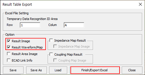
Enable the Result Image checkbox.
Enable the Result Waveform checkbox.
Click Finish/Export Excel to start Excel report
creation.
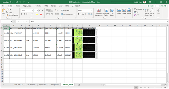
Figure 53. PollEx DFE+ begins generating an Excel report.
After running, PollEx DFE+ shows the Excel report
file. Figure 54.
 to
search and select the Memory.ibs file from
C:\ProgramData\altair\PollEx\<version>\Examples\Verification\DFEP\Simulation_Model
for DDR3 Memory device.
to
search and select the Memory.ibs file from
C:\ProgramData\altair\PollEx\<version>\Examples\Verification\DFEP\Simulation_Model
for DDR3 Memory device.
 for the Functional Type and select Resistor.
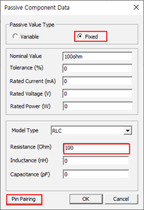
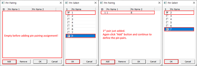
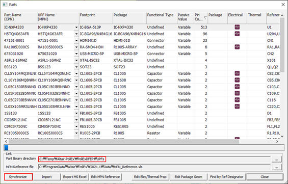
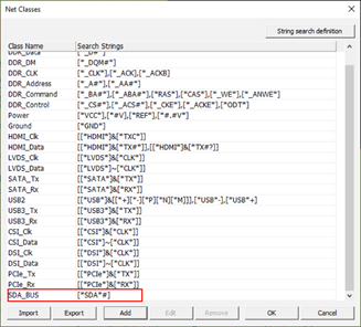
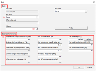
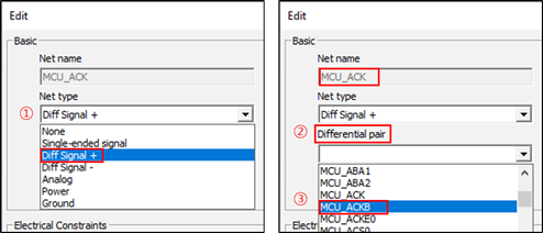
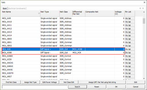
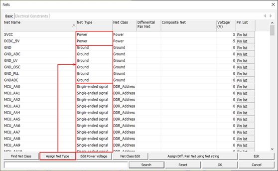
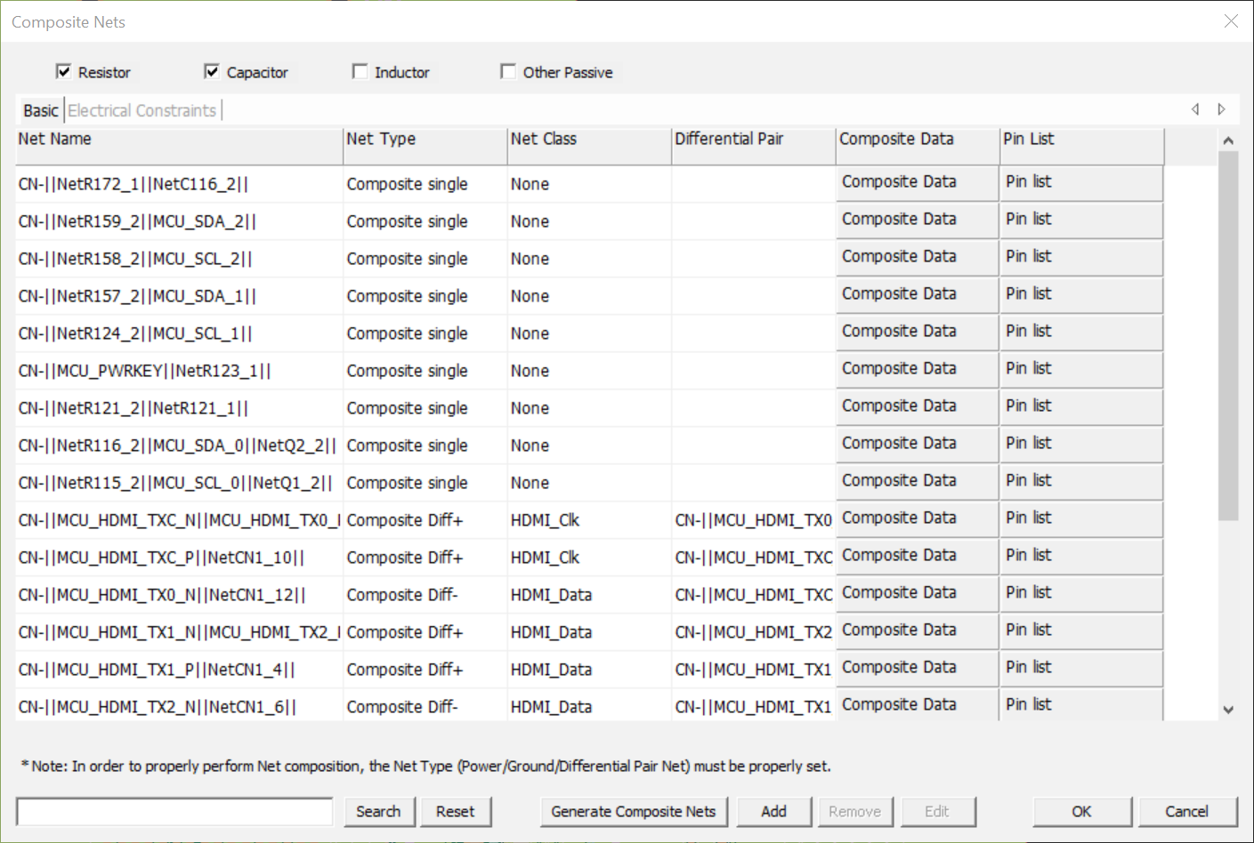 Figure 19.
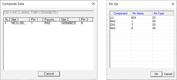
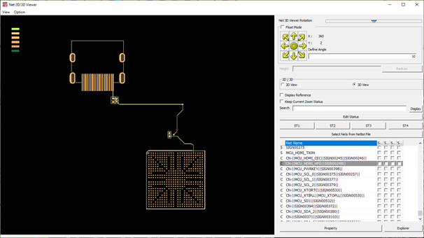
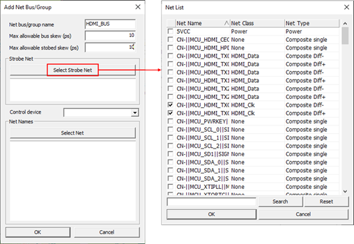
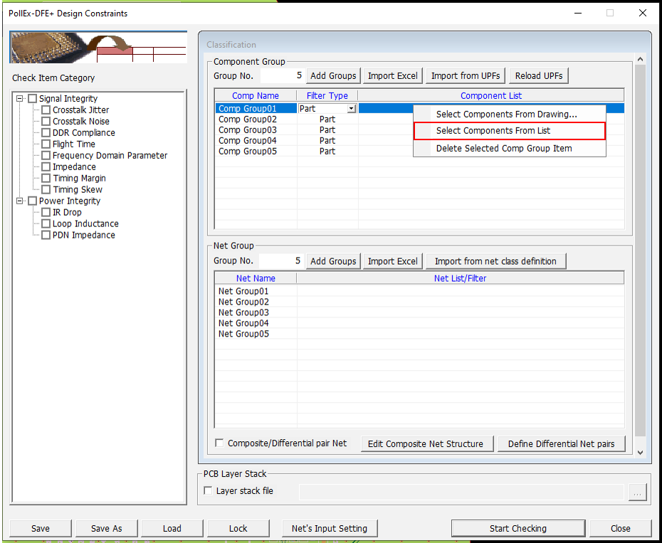 Figure 23.
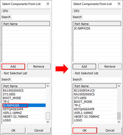
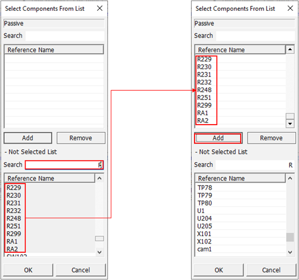
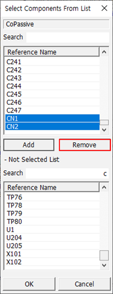
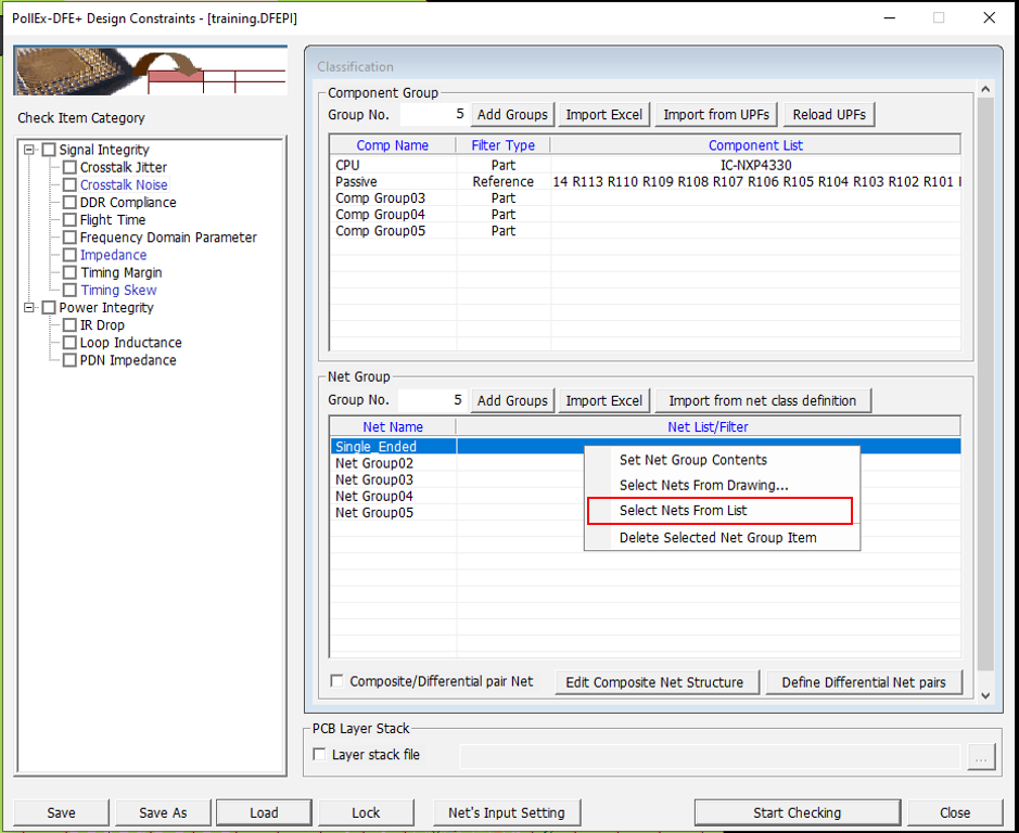 Figure 27.
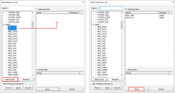
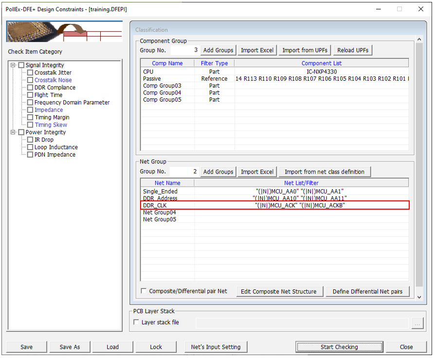 Figure 29.
 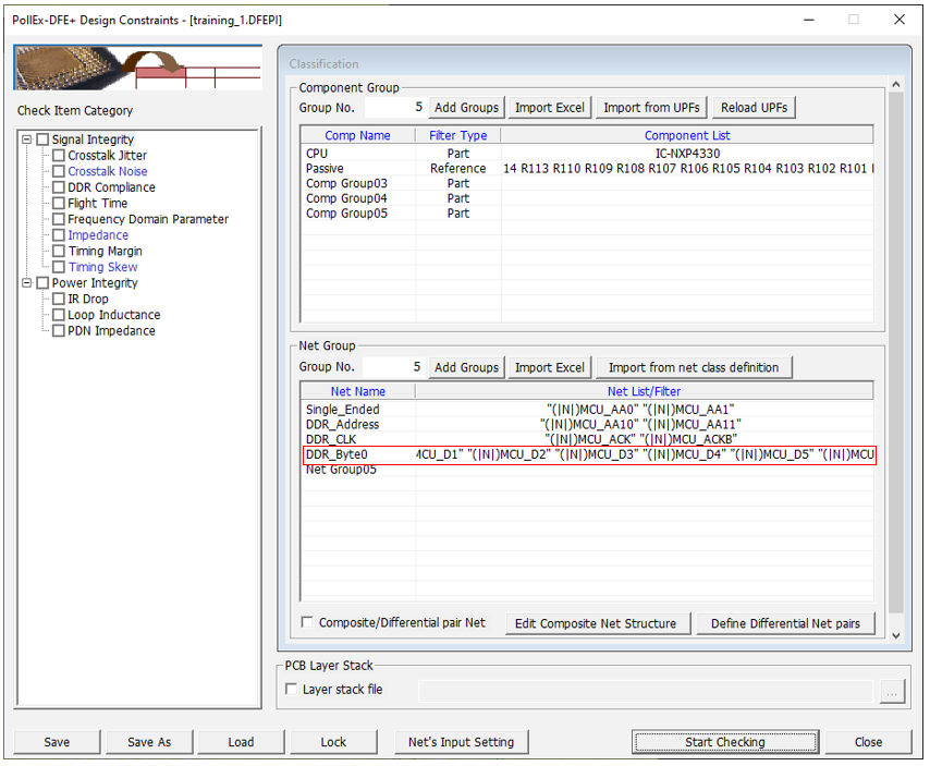 Figure 30.
 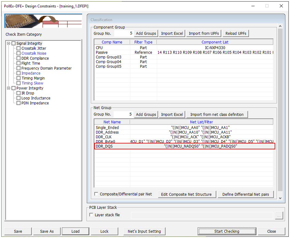 Figure 31.
 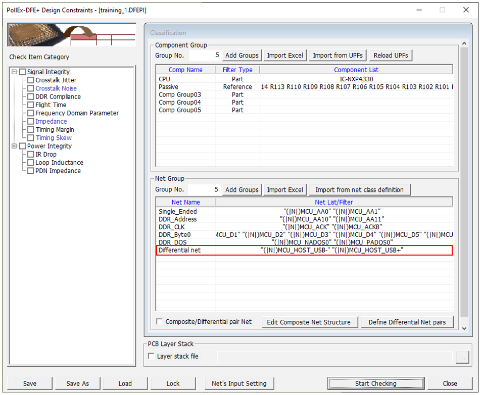 Figure 32.
 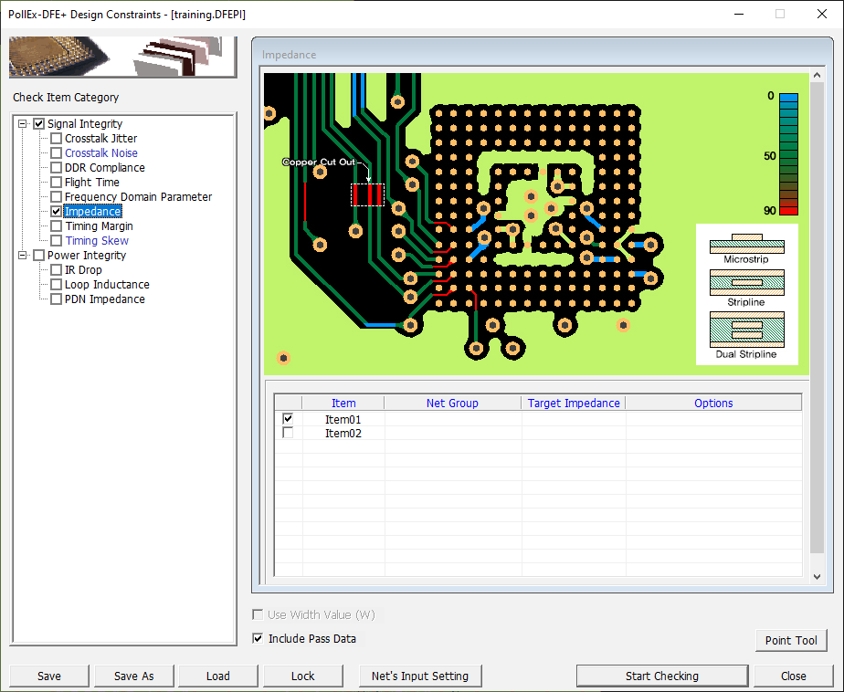 Figure 33.
 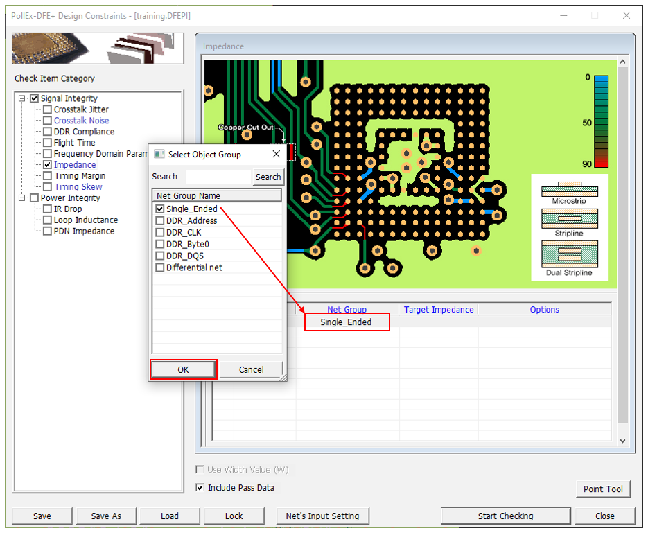 Figure 34.
 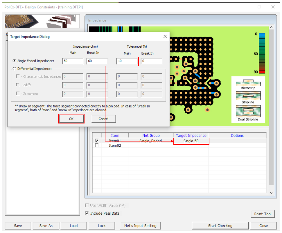 Figure 35.
 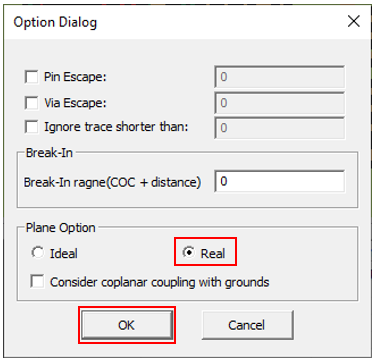 Figure 36.
 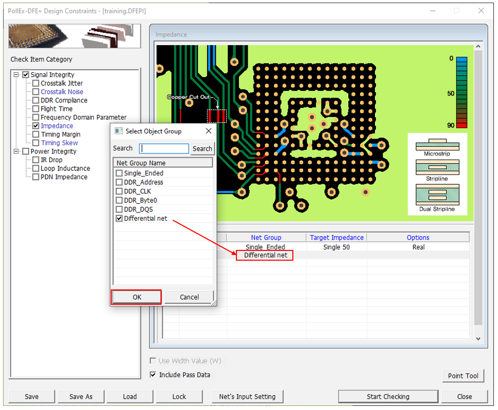 Figure 37.
 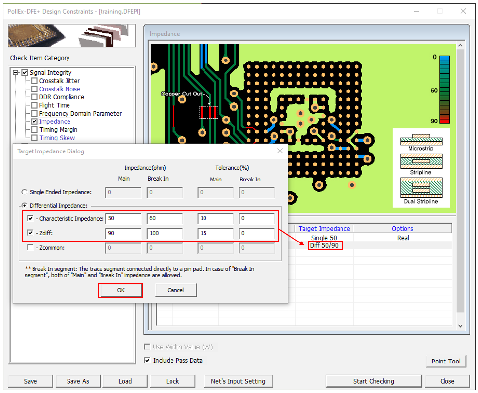 Figure 38.
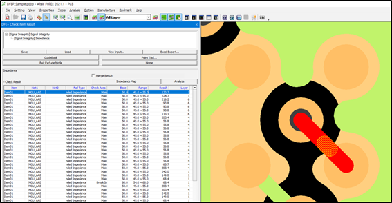
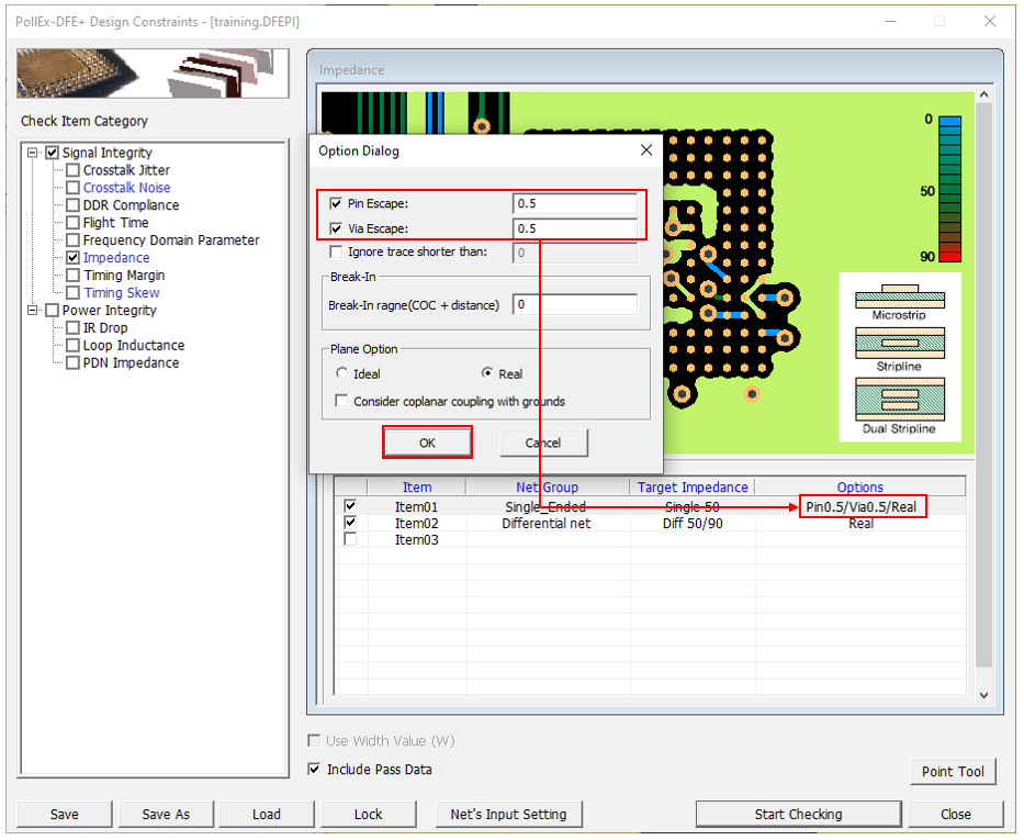 Figure 41.
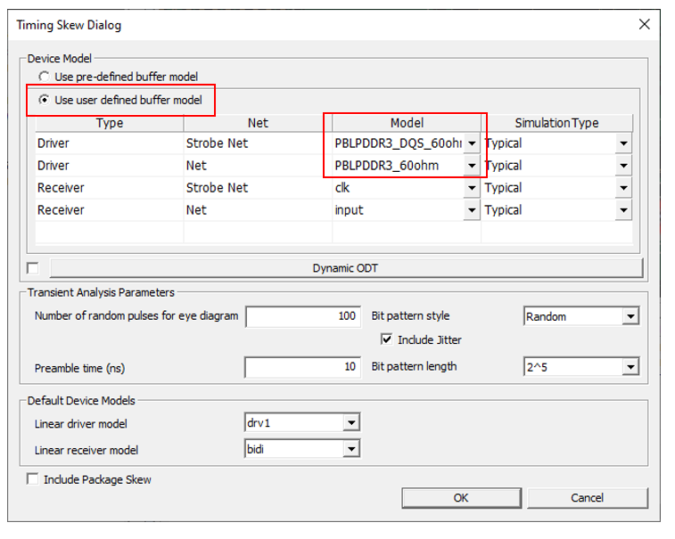
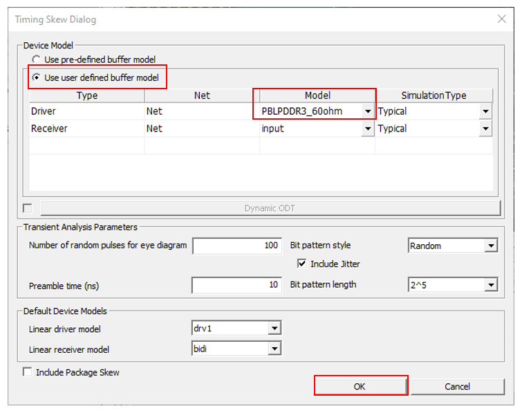
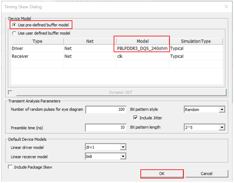
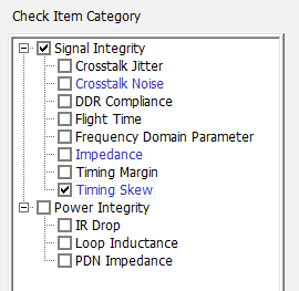 Figure 45.
  Figure 46.
  Figure 47.
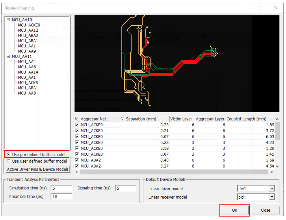
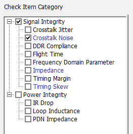 Figure 49.