PollEx DFE is one of many PollEx
toolsets and it checks electrical validity of PCB design. PollEx DFE can be launched within PollEx PCB and it helps designers to reduce design errors that
may be detected later in electrical test processes. The PollEx DFE results can be outputted to a well-formatted MS/Excel
spreadsheet. With a vast variety of user-friendly electrical rule checking options,
PollEx DFE helps you to reduce cost and time to produce
good working PCBs fast.
This tutorial is primarily designed to enable you to get a quick start with the
PollEx DFE tool. It is not intended to be a complete
reference guide for all the available test items but will give you an overview of
key concepts. Understanding these concepts will allow you to learn how to use this
tool efficiently with the help of the online documentation. Access the help by
pressing the F1 key.
This tutorial shows simple design verification flow using PollEx DFE with fairly simple design. Studying this example
carefully will help you become familiar with the PollEx DFE
tool.
In this section, you will check if high speed signals cross over split plane, and
check DDR bus robustness.
After downloading the file, uncompress the file and save it into a folder. That file
saving folder is the job folder in this tutorial.
Open and Preview PCB Design
In this step, you will open a design file in PollEx PCB and
preview PCB design.
From the menu bar, click File > Open and open the
PollEx_PCB_Sample_r<revision_number>.pdbb
file from
C:\ProgramData\Altair\PollEx\<version>\Examples\PollEx_PCB_Sample_r<revision_number>.pdbb.
Preview the PCB design.
From the menu bar, click Option > DFE > Input to open PollEx DFE.
The PollEx DFE Input dialog displays.
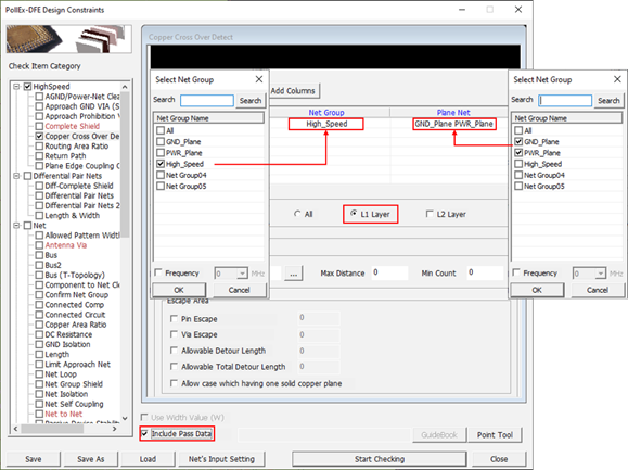
Check Copper Cross Over Detect
Activate the Copper Cross Over Detect checkbox.
The Copper Cross Over Detect dialog displays.
To
check if high speed signal cross over split plane, you will define
power/ground net group and define target net group, high-speed net
group.
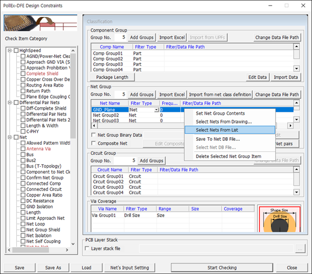
Click the classification menu.
The PollEx DFE Input dialog displays.
Define GND_Plane net group.
In the Net Group Type section, double-click Net
Group01 and change the group name to
GND_Plane by double-clicking the
Name column.
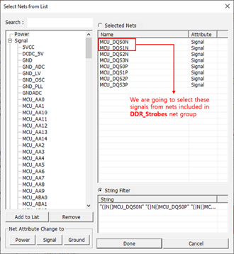
Select Select Nets From List from the context menu.
Figure 1.
The Select Nets from List dialog
displays.
Select the following multiple nets from the net list:
GND, GND_ADC,
GND_LV, GND_OSC,
GND_PLL, and
GNDADC.
Those signals are plane type ground signals that can be a reference
plane.
Click Add to List to add selected net lists to
selected items.
Click Done.
The selected list registers as a net group with the name
GND_Plane. Figure 2.
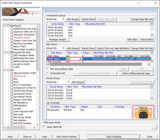
Define PWR_Plane net group.
In the Net Group Type section, double-click Net
Group02 and change the group name to PWR_Plane by
double-clicking the Name column.
Select the Select Nets From List from the
context menu.
The Select Nets from List dialog opens. Figure 3.
Select the following multiple nets from the net list:
VCC3P3_SYS,
VCC_1P5_DDR,
VCC1P5_SYS,
VCC1P0_CORE,
VCC1P0_USB, and
VCC1P2_HSIC.
Those signals are plane type power signals that can be a reference
plane.
Click Add to List to add selected net lists to
the selected item.
Click Done.
The selected list registers as a net class with the name,
PWR_Plane. Figure 4.
Define High-Speed net group.
In the Net Group Type section, double-click Net
Group03 and change the group name to
High_Speed by double-clicking the
Name column.
Select Selected Nets From List from the context menu.
The Select Nets from List dialog opens. Figure 5.
Select high speed nets from the signal net list.
The following nets are considered as high-speed signal.
MCU_SCL_0
MCU_ACKP
MCU_ACKN
MCU_DQS0P
MCU_DQS0N
Click Add to List to add the selected net list
to the selected item.
Click Done.
The selected list registers as a net class with the name, High_Speed.
There are now three required net groups: GND_Plane, PWR_Plane, and
High-Speed.
Activate the Copper Cross Over Detect checkbox to set
test condition.
The Copper Cross Over Detect Item Rule Entry dialog
opens.
Set Copper Cross Over Detect test condition.
Double-click the Net Group field.
The Select Net Group dialog should be
visible.
Select High-Speed net group, then click OK.
Double-click the Plane Net field.
The Select Net Group dialog should be
visible.
Select GND_Plane and
PWR_Plane net groups and click
OK.
Select L1 Layer in the Check Layer section to
check one layer above and below.
Activate Include Pass Data.
The passed items are also reported in addition to the failed
items. Figure 6.
With this setting, PollEx DFE will check if MCU_SCL_0,
MCU_DQS0P/N, MCU_ACKP/N signals cross over ground plane or power plane
split. The passed items are also reported in addition to the failed
items.
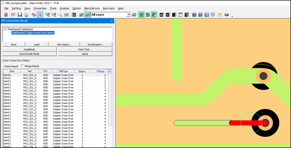
Run Copper Cross Over Detect Item and review Check Result.
Click Save As and save this input file as
training.DFESI in the
PollExDFE folder under job folder.
Note: Click Load to reload
this input setup condition.
Click Start Checking.
PollEx DFE starts checking for selected
checking items. After running, PollEx DFE
changes its window for results display.
In the result tab, select Copper Cross over
Detect and choose the first error checking item.
Figure 7.
In the right window, an enlarged image of the error area is
displayed. The cyan colored circle is the point where the error
occurred.
In the result tab, choose the second error checking item.
MCU_SCL_0 signal cross over GND plane split area at Layer2. Figure 8.
The second error case is that net cross-over plane split area,
and first error case is that net cross-over anti-pad area of
itself.
You can ignore first error case by using the PIN/VIA
Escape option.
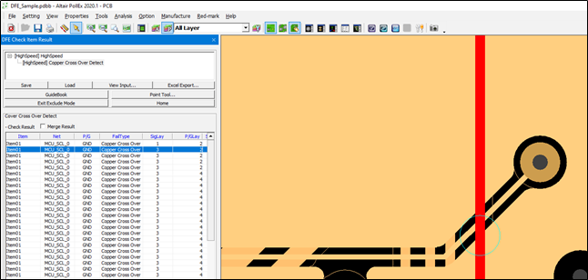
In the result tab, click View Input.
Activate Copper Cross Over Detect in the Check
Item Category section to set test condition.
The Copper Cross Over Detect dialog
displays again.
Activate PIN/VIA Escape and assign value
0.5 to exclude pin and via anti-pad area of
target signal itself.
With this input condition, if target nets cross over the anti-pad of
target signal smaller than 0.5mm will be ignored.
Click Start Checking.
Click Save.
PollEx DFE starts checking with new
input condition. After running, PollEx DFE
changes its window for results to display.
In the result tab, select Copper Cross over
Detect and choose the first error checking item.
The first case error is removed.
Select other checked items and review the results the same way.
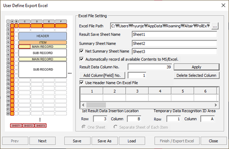
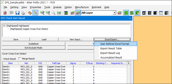
Create Excel Report
In this step, you will create an Excel report for the result.
PollEx DFE has a feature to make
a report for checking results into a file.
Click Excel Export and select User Defined
Excel Format.
Figure 9.
The User Defined Export Excel dialog displays.
Page1 settings.
Set Excel File Path.
Click Load and open the
training.DFEE file from
C:\ProgramData\altair\PollEx\<version>\Examples\Verification\DFE\DFEE
Or, you can select your own format by clicking . You will use the default excel
format.
Select Net Summary Sheet Name for net summary
reporting.
Select Automatically record all available Contents to
MS/Excel.
Enter 39 for Result Data Column No., and click
Apply to
extend the column count to 39.
Select User Header Name On Excel File.
In the User Defined Export Excel dialog, your
settings should now look as follows: Figure 10.
Click Next.
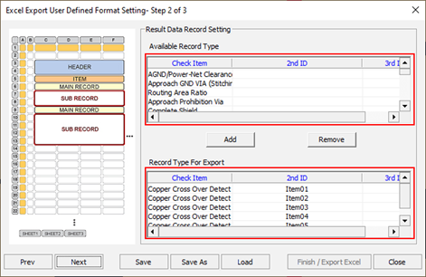
Page2 Setting.
The next step is to set excel row format. The upper section shows the total
available result items. The lower section shows the selected item for excel
report. You can choose the required item from the upper section window list, and
click ADD to move the selected item into the lower
section window. Since you already selected Automatically record all
available Contents to MS/Excel, other settings can be left
unchanged. Figure 11.
Click Next.
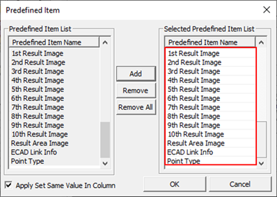
Page3 settings.
The next step is to set the excel column format. You can set the contents to
be saved in the columns of the Excel report.
Select Predefined Item to set the column with
PollEx pre-defined items, and click Set Predefined Item
List.
Select all items named BLANK, and remove them by
clicking Remove All.
Select all items available in the left section of the dialog, except
the first item named [BLANK], and click
Add.
Activate Apply Set Same Value in the
Column.
Your settings should now look as follows: Figure 12.
Click OK to close the
Predefined Item dialog.
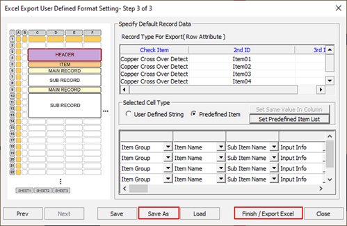
The User Defined Export Excel dialog should now
look as follows: Figure 13.
Click Save As and save the report setup
environment file as training.DFEE in the
PollExDFE folder under job folder.
You can reload this report setup condition by clicking
Load.
Click Finish/Export Excel to start the excel
report creation.
PollEx DFE starts generating the excel
report. The PollEx DFE shows the excel report
file.
Save the excel file with a different name.
It is better to keep the sample excel format file for future
use.
Check Bus2
Click View Input to open the Input
Setting dialog.
The PollEx DFE Input dialog displays.
Activate Bus2 in the Check Item Category list.
The Bus2 Item Rule Entry dialog
displays.
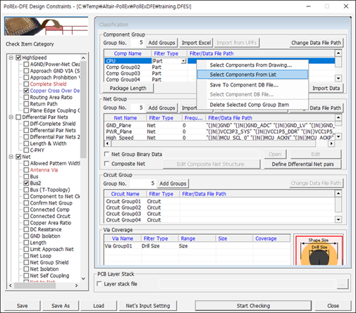
Define Component groups.
To set component groups, you will use the PollEx DFE
Input dialog.
In the dialog, click the classification menu above the Check Item
Category section.
Figure 14.
The PollEx DFE Input dialog
opens.
Define CPU component group.
In the Component Group Type section, click the first item,
Component Group01, and change the group name
to CPU.
Select Selected Component from List from the
context menu.
Figure 15.
The Selected Component from List dialog
opens.
Select the IC-NXP4330 component from the part
name list.
Click Add to add selected components to the
selected item.
Press OK to close
this dialog.
The selected list registers as a component group with the name
CPU.
Define Memory component group.
In the Component Group Type section, click the second item,
Component Group02, and change the group name
to Memory.
Select Selected Component from List from the
context menu.
This menu shows you the part list.
Select the component H5TQ4G63AFR from the part
name list.
Click Add to add the selected component to the
selected item.
Click OK to close
this dialog.
The selected list registers as a component group with the name
Memory.
Define DDR_Data0 net group.
In the Net Group Type section, click the fourth item, Net
Group04, and change the group name to
DDR_Data0.
Select Select Nets From List from the context menu.
This menu shows you the net list.
Select multiple nets MCU_D0~D7 and
MCU_DQM0 from the signal net list.
These signals are considered as data byte0 of DDR data bus.
Click Add to List to add the selected nets to
the selected item.
Click Done.
The selected list registers as a net group with the name
DDR_Data0.
Define DDR_Strobes net group.
In the Net Group Type section, click the fifth item, Net
Group05, and change the group name to DDR_Strobes.
Select Select Nets from List from the context menu.
This menu shows you the net list.
Select the following multiple nets from the signal net list:
MCU_DQS0P, MCU_DQS0N
MCU_DQS1P, MCU_DQS1N
MCU_DQS2P, MCU_DQS2N
MCU_DQS3P, MCU_DQS3N
These signals are strobe signals for DDR data byte0~3 bus.
Click Add to List to add the selected nets to
the selected item.
Click Done to close this dialog.
The selected list registers as a net group with the name
DDR_Strobes.
Activate Bus2 in the Check Item Category list.
The Bus2 item rule entry dialog
displays.
Set Bus2 test condition.
Double-click the Net field in the Bus2
input setup dialog to select the target net from the net
group list.
The Select Object Group dialog
displays.
Select DDR_Data0 as the target net group, then
click OK to close this
dialog.
Double-click the Base Net field in the
Bus2 input setup dialog to select strobe net
from the net group list.
The Select Object Group dialog
displays.
Select the DDR_Strobes net group as a strobe net
group and click OK.
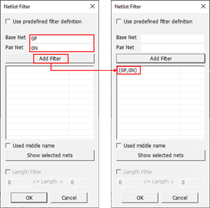
Activate the Filter option.
Double-click the Filter field in the
Bus2 input setup dialog to select MCU_DQS0P and
MCU_DQS0P among the nets included in the DRAM_Strobes net group
list.
The Netlist Filter dialog displays. Figure 16.
Enter the Base Net name filter as 0P and enter
the Pair Net name filter 0N.
Click Add Filter.
Figure 17.
Click OK.
Double-click the Start Component field in the
Bus2 input setup dialog to select
Start Component from the component group
list.
The Select Object Group dialog
opens.
Select CPU as a start component group and click
OK.
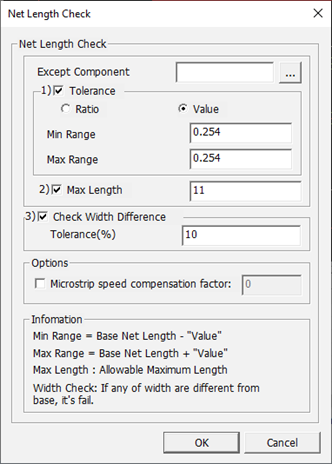
The Net Length Check condition setup.
Double-click the Net Length Check field in the
Bus2 input setup dialog to set the Net Length
Check test condition.
The Net Length Check dialog
opens.
Activate the Tolerance checkbox.
Activate the Value checkbox.
Enter the Min Range value 0.254.
Enter the Max Range value 0.254.
Activate the Max Length checkbox and enter
11 for the value.
Activate the Check Width Difference checkbox,
and enter 10 for Tolerance.
In the Net Length Check dialog, your settings
should now look as follows: Figure 18.
Click OK.
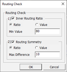
The Routing Check condition setup.
Double-click the Routing Check field in the
Bus2 input setup dialog to set the Routing
Check test condition.
The Routing Check setup dialog
opens.
Activate the Inner Routing Ratio checkbox.
Activate the Ratio checkbox.
Enter 80 for the Min Value.
Activate the Routing Symmetry checkbox.
Activate the Ratio checkbox.
Enter 10 for the Max Difference value.
In the Routing Check dialog, your settings should
now look as follows: Figure 19.
Click OK.
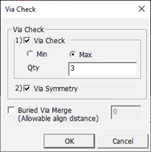
The Via Check condition setup.
Double-click the Via Check field in the
Bus2 input setup dialog to set the Via Check
test condition.
The Via Check dialog opens.
Activate the Via Check checkbox.
Activate the Max checkbox.
Enter 3 for the Qty value.
Activate the Via Symmetry checkbox.
In the Via Check dialog, your settings should now
look as follows: Figure 20.
Click OK.
With this setting, PollEx DFE checks the
following:
If the length of DDR Data byte0 nets is between DQS net length –
0.254mm and DQS net length + 0.254mm.
If the length of DDR Data byte0 nets is longer than 11mm.
If the width of DDR data byte0 nets is the same as DQS nets within
10 percent range.
If the DDR data byte0 nets are routed on inner layer over 80 percent
range.
If the inner routing ratio of DDR data byte0 nets is the same as the
inner routing ratio of DQS nets within 10 percent range.
If the via count of DDR data byte0 and DQS nets is greater than
three.
If the via count of each DDR data byte0 nets and DQS nets is the
same.
Run Bus2 Item and review Check Result.
Unselect the Copper Cross over Detect test items
in the Check Item Category section.
Click Start Checking.
PollEx DFE will ask you to save the current
input file status or not.
Click Save to save the current setup.
PollEx DFE starts checking for the
selected checking items. After running, PollEx DFE changes its window for results
display.
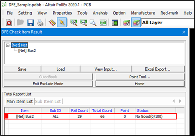
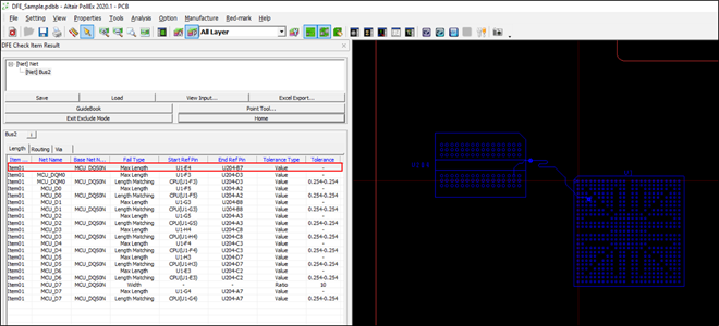
In the result tab, click [Net]Bus2 to see the
detailed result.
Figure 21.
Review Net Length Check Result.
Click Length to review the length check
result.
Choose the first error checking item of this section.
You can see the error occurring location and its picture. You can also
see that the trace length of MCU_DQS0N net is 19.721mm. It is longer
than the limit 11mm, so it fails. Figure 22.
Click Routing to review the routing check
result.
Choose the first error checking item of this section.
The total routing length of MCU_DQS0N net is 19.7211mm. The required
inner routing ratio is 80 percent. To meet the required inner routing
ratio of 80 percent the inner routing length of the MCU_DQS0N net should
be longer than 15.7769mm. The inner routing length of MCU_DQS0N is
15.1205mm, so it fails.
Select other checked items and review the results the same way.

 . You will use the default excel
format.
. You will use the default excel
format.