PollEx Technical Cleanliness (TC) is an optional module of the
PollEx PCB and a reliability analyzing tool set for PCB
designs.
PollEx TC checks for visible residues called particles to
decreases short-term and long-term board problems and increase functionality. The
Checked results of PollEx TC can be exported into a well
formatted Excel spreadsheet. As a result, PollEx TC helps to
reduce defectiveness and increase productivity.
Launch PollEx PCB.
Open the PollEx PCB layout design file.
From the menu bar, click File > Open.
Navigate to the Pollex_PCB_Sample_r1.0.pdbb file
located at
C:\ProgramData\altair\PollEx\<version>\Examples
Refer to the PollEx PCB manual to use the PollEx PCB viewer.
Click Load and select the
PollEx_Sample_r1.0.teci file located at
C:\
ProgramData\altair\PollEx\<version>\Examples\Verification\TechnicalCleanliness.
Click Set Area and select the region to be
analyzed.
Figure 1.
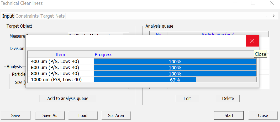
Click Start to run the Analysis.
PollEx TC checks where the design’s data input
rules and constraints apply.
Figure 2. Technical Cleanliness Analysis
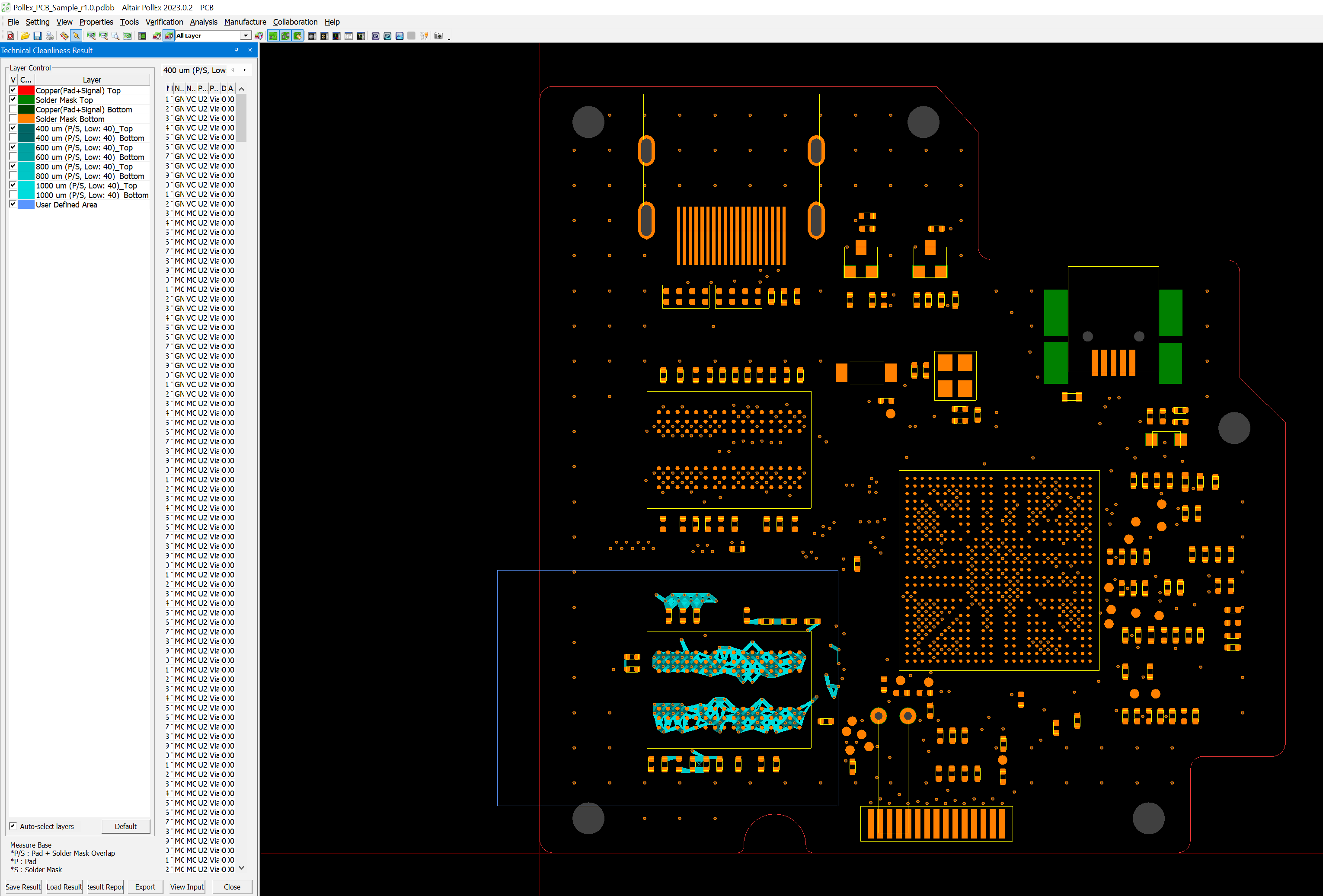
Check the results.
The test results are displayed on the screen (Particle size &
locations) after analysis. Figure 3. Technical Cleanliness Result
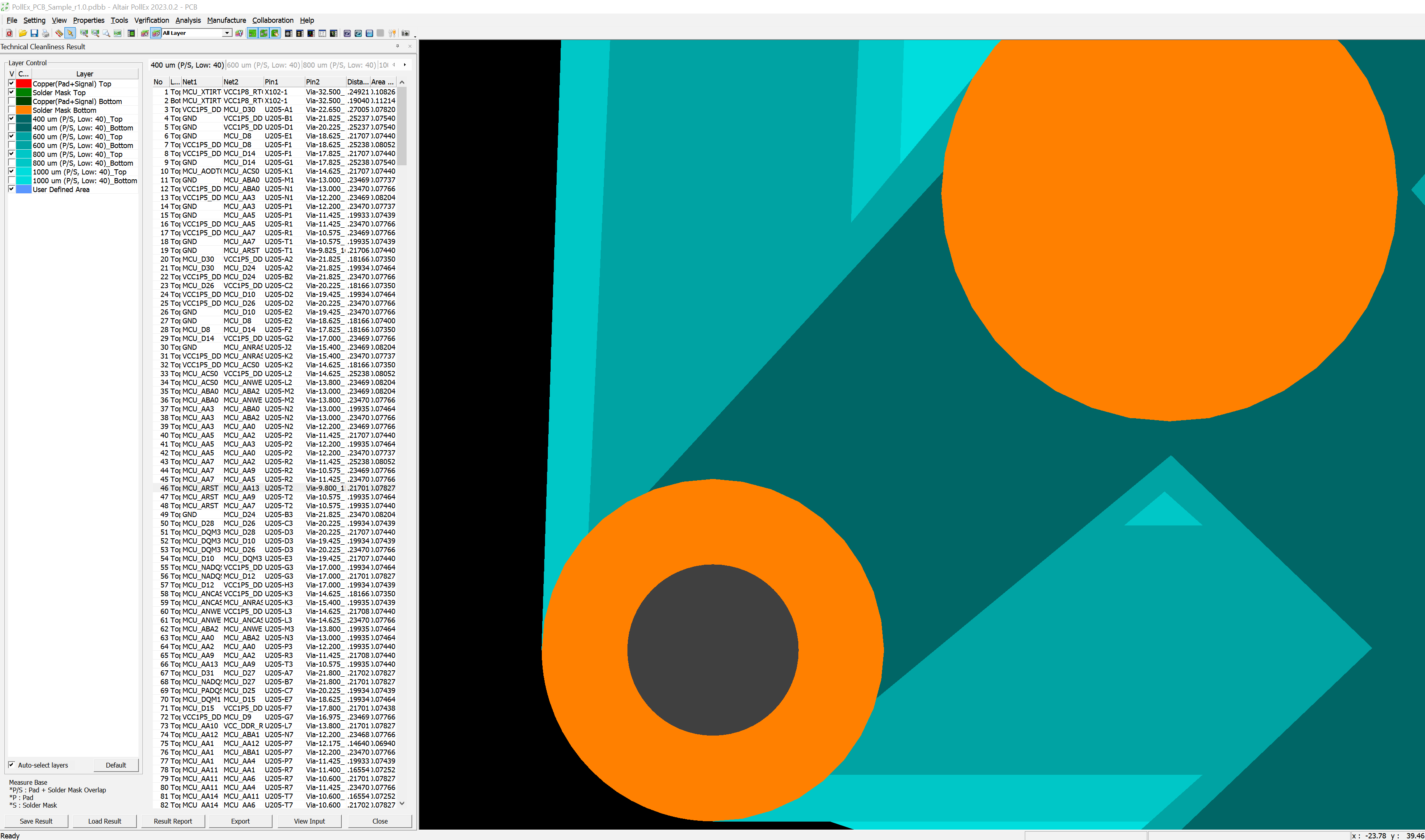
Click the 400um(low) particle size.
In the result dialog bar, you can check detailed list information of NETS and
PINS, as well as its DISTANCE and AREA. When you click an item from the list, it
displays the highlighted location with its associated layers. Figure 4.
Save Test result.
Click Save Result > Pollex_PCB_Sample_r1.0 > Save.
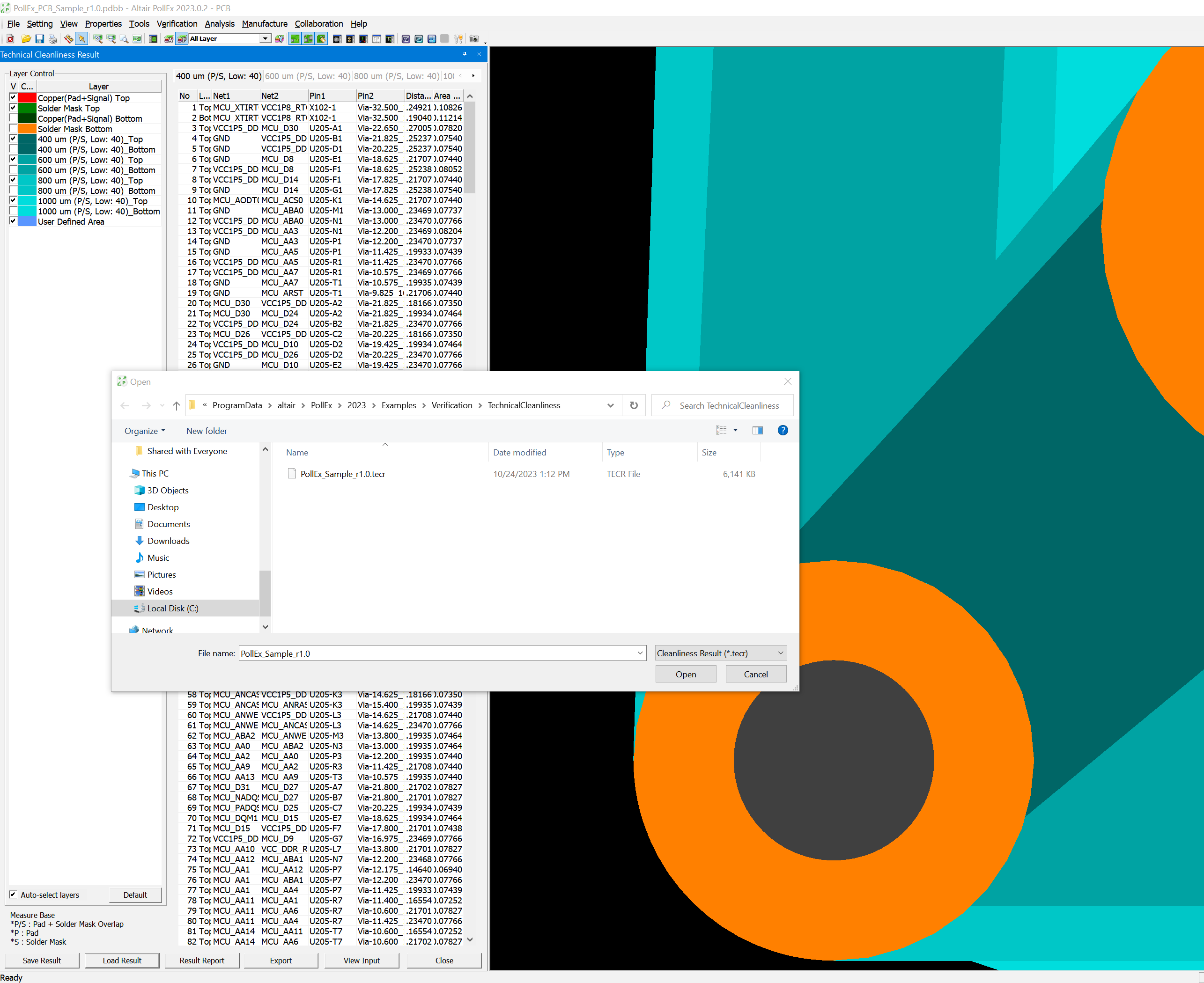
To view, click Load Result and open the
Pollex_PCB_Sample_r1.0.tecr file located at:
C:ProgramData\altair\PollEx\<version>\Examples\Verification\TechnicalCleanliness.
Figure 5.
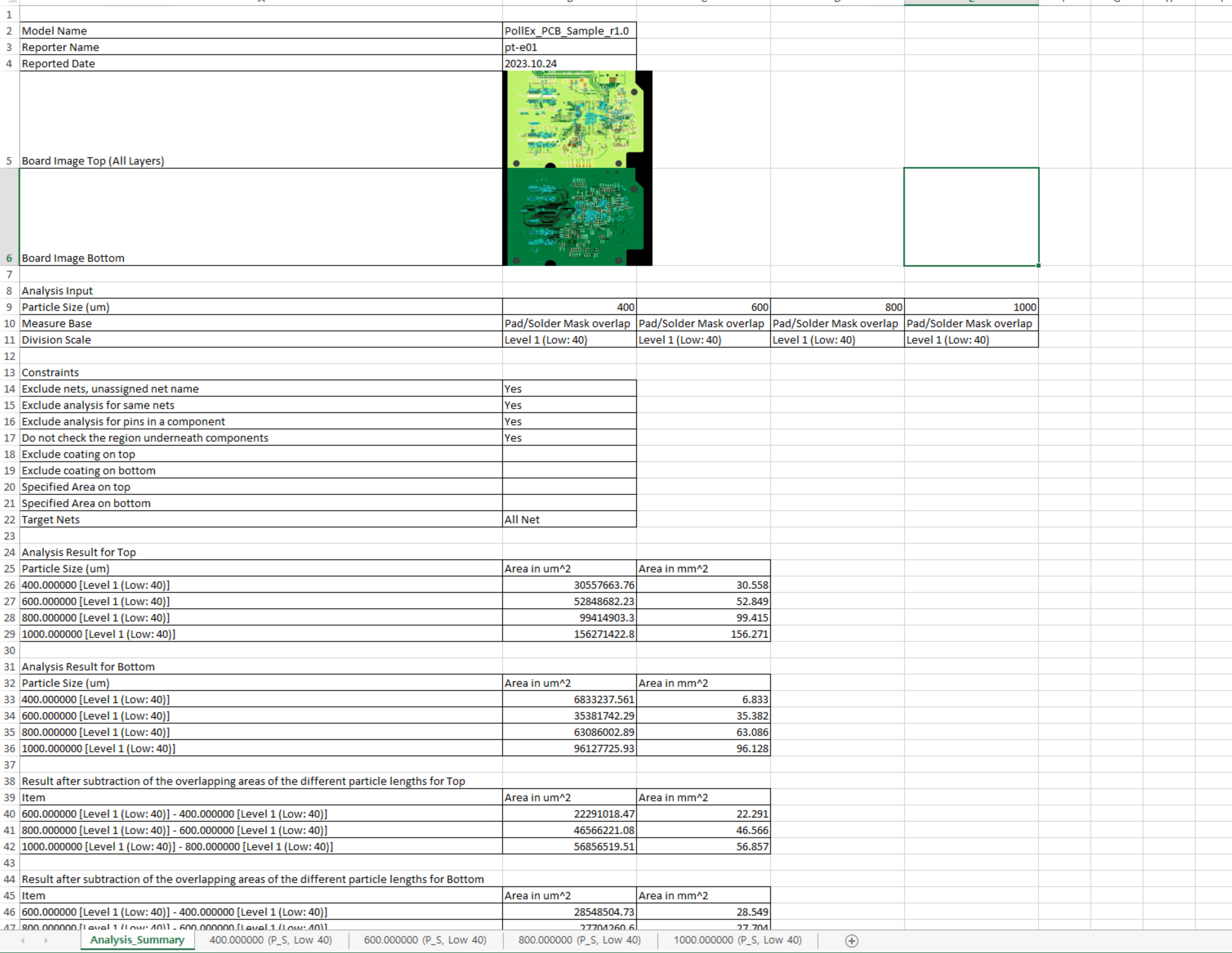
Export the Result Report.
Click Result report > File name (Pollex_PCB_Sample_r1.0) to export the result to Excel.
To view, open the Pollex_PCB_Sample_r1.0.xlsx file
located at:
C:ProgramData\altair\PollEx\<version>\Examples\Verification\TechnicalCleanliness.
Figure 6. Result Report
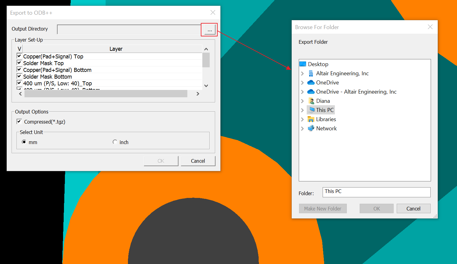
Export to ODB++ Format
Click Export
Select the Output Directory, Set Layers to Export and Unit of the
Design Figure 7.
To view, open the Pollex_PCB_Sample_r1.0.tgz file located at the
Selected Output Directory
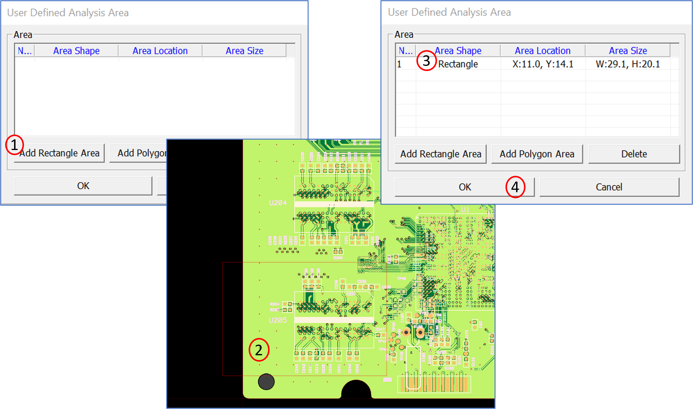 Figure 1.