Environment Setting
In this section, PollEx Environment setting methods are explained.
Setting for Local Library Database
For Signal Integrity Analysis, you can define all the default setting. From the menu bar, click . The Environment dialog opens.
Setting for Linear Model
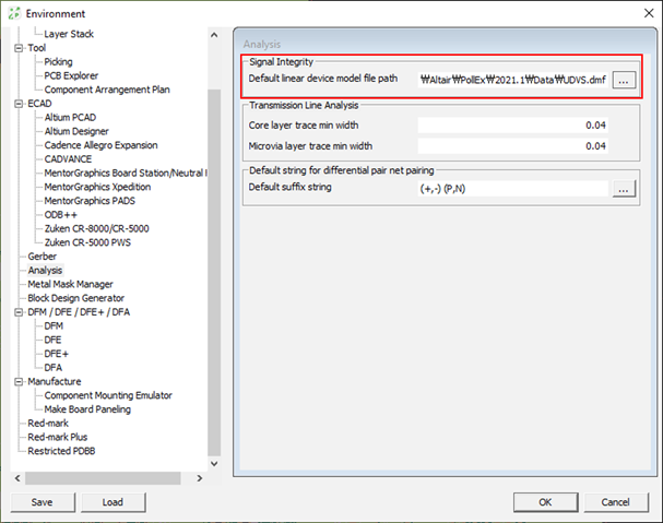
Figure 1. Default Linear Model Path Setup
IO buffer device models of input and output pins of signal nets are stored in the part data file of individual components. When the device models are not available in the part data, the default linear device models defined here are used for transient simulation of signal integrity analyses. With the use of Linear Device Modeler, you can create linear output (driver) and input (receiver) device models and store them in a linear device model file. PollEx DFE+ provides you with a system default linear device model file, UDVS.dmf.
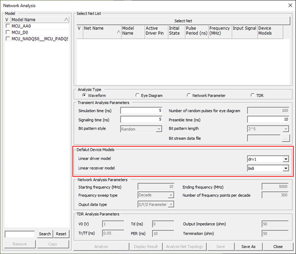
Figure 2. Default Linear Buffer Setup
Setting for Allowable Minimum Trace Width
From the Environment dialog, select Analysis to open the Analysis Environment dialog. As shown in Figure 1.
During Transmission Line Analysis, you can let the program find the trace widths whose characteristic impedance values match the target impedance values by selecting the Get Impedance Matching Trace menu.
A built-in electromagnetic field solver is employed for the calculation of characteristic impedances and finding impedance matching trace widths. Finding impedance matching trace widths is performed under the constraints of minimum signal trace widths value defined in this setting item. If an impedance matching trace width cannot be found within the constraints, you need to change layer stack properties, such as dielectric layer thickness and location of power or ground plane layer.
Core layer trace min width: Minimum trace width of PCB outer layer limited by PCB manufacturer.
Microvia layer trace min width: Minimum trace width of PCB inner layer limited by PCB manufacturer.