Add Pin Name
Add the pin name to the PCB design area.
-
Select Pin For Figure Data: When automatically creating a pin name on the PCB
design area, click the pad that is the reference point to select
it.
With the Pin Select window displayed, drag, and select the pin area to create a pin number in the drawing on the right side of the screen.
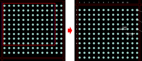
Figure 1. -
Side View: Create a side view of the BGA Ball Map.
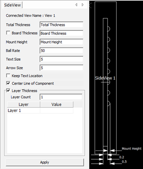
Figure 2.- Total Thickness: Enter the side thickness display value.
- Mount Height: Enter the display value.
- Ball Rate: Enter the rate of the ball protruding from the body to display in the side view.
- Text Size: Sets the text size.
- Arrow Size: Sets the size of the arrow.
- Keep Text Location: Fix the text when changing text size and arrow size.
- Center Line of Component: Displays the center line of the component.
- Layer Thickness: Applies layer thickness.
- Layer Count: Sets the number of layers to apply thickness.
- Apply: Applies the set condition.