Define Properties
From the menu bar of Metal Mask Manager, click Properties.
Reference List
From the menu bar of Metal Mask Manager, click .
The Reference List dialog contains the
following sections:
- Reference List: Components in design will be namely listed with tree
structure and if users select certain component, selected component’s pin
list will be displayed.
- Blue Reference Name: Parts with Metal Mask shape modified.
- Purple Reference Name: Parts that not generated Metal Mask by Standard Metal Mask.
- Using Auto Zoom feature, selected component and component’s pin will be highlighted and focused.
- Using component searching feature, users can find desired components.
- Property: Selected component in Reference List, pin’s detail properties will be shown.
- Edit Metal Mask: Use the menu to change the shape of selected pin in
Reference List. Click Edit Metal Mask to select
desired metal mask shape.
Figure 1. 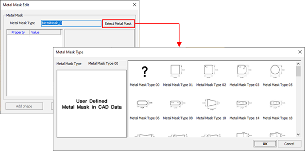
- Delete Metal Mask: Delete selected pin’s standard metal mask shape.
Layer Control
From the menu bar of Metal Mask Manager, click .
Display Option
- Normal: Default display status. Pads and metal mask shape will be solid state, so overlapped area will be not shown.
- Translucency Mode: Transparent display status. Pad and metal mask shape will be shown with transparently, so you can check the behind region of overlapped objects.
Layer
- Layer Name: Check whether the layer is displayed on Top or Bottom.
- Color: Set the layer color for Top and Bottom.
- Layer Priority: Set the display priority for each layer. The lower the number, the higher it displays.
Board Mini Map
- At this window, you can see the working area on the whole board.
- Red colored line is the board contour and yellow colored line is displaying region.
Validation Check Result
Using validation check feature, you can check the result.
From the menu bar of Metal Mask Manager, click . The Validation Check Report dialog opens.
The Validation Check Report dialog contains the following sections:
- Layer: For checking results, you can display by layers among all, top, or bottom.
- Highlight Component: Make highlight for selected component in checking result.
- Same Padstack Merge: For the same padstack, this option shows them per reference designators.
- Reference Name: Reference names that failed from the checking.
- Part Name: Part name that failed from the checking.
- Pin Name: Pin name that failed from the checking.
- Layer: Layer that failed from the checking.
- Fail Type: Fail types.
- Shape: In case of metal mask shapes are different.
- Gerber X: In case of Gerber file doesn’t have matching metal mask.
- Gerber O: In case of Gerber file has unnecessary metal mask.
- BOM: In case of components are not in BOM having metal mask in Gerber file.
- Pin Location X/Y: Pin X/Y location.
- Standard DB Name: Component DB which is having fails.
- Padstack Name: Padstack’s name which is having fails.
- Padsize (Width/Length): The size of padstack which has fails.
- Standard Padsize (Width/Length): User-created padstack size. If metal mask DB has no standard pad size, this column will be NONE.
- View Standard DB: You can review failed component’s standard metal mask for which components are having fails.
- View Part: For components having fails, you can review components with PollEx PCB’s part viewer.
Validation Pin Pitch Check Result
From the menu bar of Metal Mask Manager, click .
The Validation Pin Pitch Check Report contains the following sections:
- Reference Name: Reference name of component which is having fails.
- Part Name: Part name of component having fails.
- Pin Pitch: The pitch of pin having fails.
- Standard Pin Pitch: Shows standard pin pitch.
- Standard DB Name: Shows component DB name in which component having fails belong to.
- View Standard DB: You can review standard mask shape of component having fails.
- View Part: You can review component having fails using PollEx PCB’s part viewer.
Gerber Layer Setting
From the menu bar of Metal Mask Manager, click .
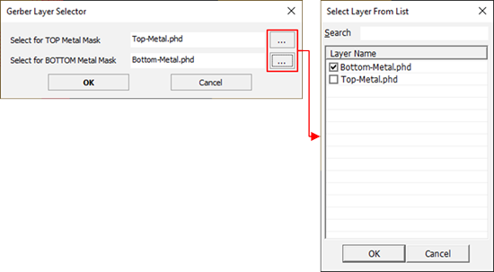
- Select for TOP Metal Mask: Set top layer of reading Gerber file.
- Select for BOTTOM Metal Mask: Set bottom layer of reading Gerber file.