Under Hole/Via
Check the via or hole under special components.
Under some components, placement is not allowed for vias or holes.
The Under Hole/Via dialog contains the following
sections:
- Laser Via Definition: Define the laser via.
- Maximum Hole Size: Set the maximum via hole size.
- Via Selection from Library: Select a laser via from the library in the design.
- Checking: Under specified component, another via or hole cannot be
placed.
- All Components: Set all placed components as target.
- Checking Area Definition: Set the components area where the
other vias or holes should not be placed.
Figure 1. 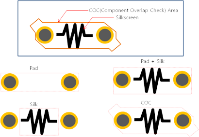
- COC: Area defined in component overlap check (COC) area.
- Silk: Area including silkscreen.
- Silk + Pad: Area including pad and silkscreen area.
- Pad: Area including pads.
- COC + Pad: Area defined in pad and COC area.
- Center: Check based on the center point of the part.
- Default: Use the component area basement used in the default setup in the Component Classification Setting dialog. If it is undefined in the Component Classification Setting dialog, pad including area will be used as default.
- Checking Layer Definition
- All: PollEx DFM checks for top and bottom.
- Component Placed Layer: PollEx DFM checks only for the target component placed layer.
- Basement of Vias: You can set a via measurement base for
measuring distance from a via.
Figure 2. 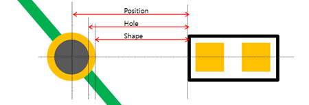
- Position: Via location.
- Shape: Via outer pad shape.
- Hole: Via hole outer size.
- Option
- Except for GND Connected Via: Even if a via are
detected by PollEx DFM, if
it is a ground via, it does not fail.
- Select GND Net: Select ground net from net list.
- Exclude Vias in Thermal Copper Area or BGA Pad Area: Even if vias are detected by PollEx DFM, if they are vias in thermal copper-pour or under BGA packages pad, they do not fail.
- Except for Silk Covered Via: Exclude via that is covered with Silkscreen.
- Expand Area: Set the clearance area.
- Horizontal: Set the clearance horizontal area.
- Vertical: Set the clearance vertical area.
- Except for GND Connected Via: Even if a via are
detected by PollEx DFM, if
it is a ground via, it does not fail.
- Checking Target Object Definition
- Hole: If holes exist under specified components, PollEx DFM defines them as fails.
- Through Via: If through vias exist under specified components, PollEx DFM defines them as fails.
- Inner Via: If inner vias exist under specified components, PollEx DFM defines them as fails.
- Laser Via: If laser vias exist under specified components, PollEx DFM defines them as fails.
- Padstack String Filter: If using string filter vias
exist under specified components, PollEx DFM defines them as fails.
- Import(.txt): Apply Filter Type based on the
characters entered in the .txt file.
- Apply as a prefix when (|F|) ABC is entered in the .txt file.
- Apply as a mid-string when ABC is entered in the .txt file.
- Apply as a suffix when ABC(|P|) is entered in the .txt file.
- Export(.txt): Export the characters registered in the String Item in .txt file format.
- Import(.txt): Apply Filter Type based on the
characters entered in the .txt file.
- Checking Area Definition: Set the components area where the
other vias or holes should not be placed.
- Component Group Selection: Select the target components as a group
selection from the list.
Figure 3. 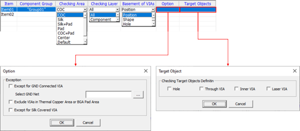
- Item: Specify the item name.
- Component Group: Select target component group from the list.
- Checking Area: Set the component area where other vias or
holes should not be placed.
Figure 4.
- COC: Area defined in COC area.
- Silk: Area including silkscreen.
- Silk + Pad: Area including pad and silkscreen area.
- Pad: Area including pads.
- COC + Pad: Area defined in pad and COC area.
- Center: Check based on the center point of the part.
- Default: Use the component area basement used in the default setup in the Component Classification Setting dialog. If it is undefined in the Component Classification Setting dialog, the pad including area will be used as default.
- Checking Layer:
- All: PollEx DFM checks for top and bottom.
- Component Placed Layer: PollEx DFM checks only for the target component placed layer.
- Basement of Vias: You can set a via measurement base in
measuring distance from a via.
Figure 5.
- Position: Via location.
- Shape: Via outer pad shape.
- Hole: Via hole outer size.
- Option
- Except for GND Connected Via: Even if vias are detected by PollEx DFM, if they are ground vias, they do not fail.
- Select GND Net: Select ground net from net list.
- Exclude Vias in Thermal Copper Area or BGA Pad Area: Even if vias are detected by PollEx DFM, if they are vias in thermal copper-pour or under BGA packages pad, they do not fail.
- Except for Silk Covered Via: Exclude via that is covered with Silkscreen.
- Expand Area: Set the clearance area.
- Horizontal: Set the clearance horizontal area.
- Vertical: Set the clearance vertical area.
- Target Objects
- Hole: If holes exist under specified components, PollEx DFM defines them as fails.
- Through Via: If through vias exist under specified components, PollEx DFM defines them as fails.
- Inner Via: If inner vias exist under specified components, PollEx DFM defines them as fails.
- Laser Via: If laser vias exist under specified components, PollEx DFM defines them as fails.
- Padstack String Filter: If using string filter vias
exist under specified components, PollEx DFM defines them as
fails.
- Import(.txt): Apply Filter Type based on the
characters entered in the .txt file.
- Apply as a prefix when (|F|) ABC is entered in the .txt file.
- Apply as a mid-string when ABC is entered in the .txt file.
- Apply as a suffix when ABC(|P|) is entered in the .txt file.
- Export(.txt): Export the characters registered in the String Item in .txt file format.
- Import(.txt): Apply Filter Type based on the
characters entered in the .txt file.
- Except Component Group Selection: Set the void-checking component group.
- Slit hole existence check: Check for the presence of a slit hole within the component.
- Hole Layer Definition: Set the slit hole layer.
- Component Area: Check if there is a slit hole within the
area of the component.
- Item: Specify the item name.
- Component Group: Select target component group from the list.
- Check Type: Select check type.
- Component Center: Check if the slit hole exists at the center of the component.
- Component Area: Check if the slit hole exists within the component.
- Measure Base: Set the target component measurement base.
- Expand Comp Area: Set the acceptance range for the slit hole. The component expands based on the area edge criteria, and if the slit hole exceeds the set value, it will pass.
- Slit Hole Width: Set the Slit Hole thickness. If the Slit Hole thickness exceeds the set value, it will result in a Pass.
- Between Pins: Check for the presence of a slit hole between
the pins.
- Item: Specify the item name.
- Component Group: Select target component group from the list.
- Pin Measure Base: Select the pin measurement base.
- Pin Distance: Set the pin distance. If there is no slit hole at the set distance, it will be detected as a fail.
- Slit Hole Width: Set the Slit Hole thickness. If the Slit Hole thickness exceeds the set value, it will result in a Pass.
- Component Area: Check if there is a slit hole within the
area of the component.
- All Components: Set all placed components as target.