Power-Net to Net
The rule checks whether two power traces have enough spaces.
- Auto Net to Net Combination: Generate combination pair of selected net group.
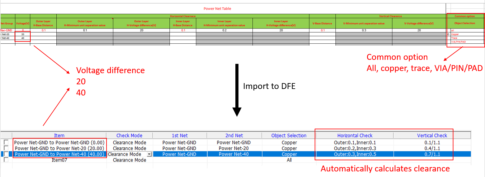
- Import Power-net clearance excel table: Import excel table that
automatically calculates vertical and horizontal clearance based on the
difference in voltage. The user can define the voltage difference and its
corresponding clearance value as required. In the figure below, the user has
set up to get 0.1mm clearance for every 20 voltage difference. The vertical
and horizontal clearance values are automatically calculated and imported
based on this setup.
- Default Check Mode: Select a method to check separation between nets.
- Clearance Mode: Check the separation by segment of the net.
- Expand Mode: After expanding Net1 to the required separation, check for overlap with Net2.
- Item: Enter item name.
- 1st Net: Select a reference power net group.
- 2nd Net: Select a target power net group. The DFE checks the clearance between 1st Net and 2nd Net.
- Exclude Composite: If selected, for Composite Net, DFE disassemble it and examine only the Base Net.
- Object Selection: Define in detail the object to be tested (All/Copper/Trace/VIA/PAD).
- Horizontal check: Setup horizontal check option.
- Power Net Clearance Check (Horizontal): Assign a reference horizontal clearance value for MS and S/L structure.
- Options
- Consider Hole Effect: Define special test conditions when
holes exist between nets.
- Hole Size Factor: If a hole is placed between two nets, assign a hole size factor. If a hole exists between two nets, the effective distance is Distance X Hole Size Factor.
- Ignore holes smaller than: : If the width of the hole between nets is smaller than this value, the hole size factor is not applied.
- Check minimum detour length: If there are holes between nets, and if the detour length of both ends of the hole is less than this value, the result is failed.
- Consider solder resist opened PADS: After assembling the
PBA, the top of the PAD is covered with solder, so the size
of the PAD is slightly larger. If this option is used,
effective PAD size is used during check. You can assign
factors differently depending on whether the component is
SMD or DIP.
- Extend range from PADs: The distance to be extended.
- Pin Escape: Enter a radius of circular region around pins to be excluded for the rule check.
- Include Pad: DFE will check net separation including PAD. You can designate the component type to which this option is applied.
- Exclude segment (width): Make exceptions to the test for segments with a specific width.
- Consider Hole Effect: Define special test conditions when
holes exist between nets.
- Vertical Check: Setup vertical check.
- Power Net Clearance Check (Vertical): Assign a reference vertical
clearance value.
- Minimum vertical clearance: Assign minimum required vertical clearance.
- Maximum allowable overlapped area size: If the plane overlaps vertically, it is regarded as fail if the overlapped area is larger than this value.
- Exclude if a distance to other layer is greater than: If the distance between the two layers is farther than this value, vertical clearance is not checked between these two layers.
- Include Pad: DFE checks net separation including PAD.You can designate the component type to which this option is applied.
- Exclude segment (width): You can make exceptions to the test for segments with a specific width.
- Consider Hole Effect: Define special test conditions when holes
exist between nets.
- Hole Size Factor: If a hole is placed between two nets, assign a hole size factor. If a hole exists between two nets, the effective distance is Distance X Hole Size Factor.
- Ignore holes smaller than: : If the width of the hole between nets is smaller than this value, the hole size factor is not applied.
- Power Net Clearance Check (Vertical): Assign a reference vertical
clearance value.
Example
In order to reduce power trace coupling, it is best to make wider clearances for trace. However, clearances are restricted by board size and pin pitch as well as power characteristics such as voltage or current. For example, a clearance among high current power is usually wider than that among normal power nets. A clearance between high power and normal power is also wider than that among normal power nets.
Clearances among power nets must be carefully considered on the same layer as well as on adjacent layers.
| Voltage (DC or AC Peak) | Minimum distance (uncoated) | Minimum distance (uncoated) | ||
|---|---|---|---|---|
| ~ 15V | 15 mil | 0.4 mil | 5 mil | 0.13 mil |
| 15V ~ 30V | 15 mil | 0.4 mil | 10 mil | 0.25 mil |
| 30V ~ 50V | 15 mil | 0.4 mil | 15 mil | 0.4 mil |
| 50V ~ 100V | 25 mil | 0.6 mil | 20 mil | 0.5 mil |
| 100V ~ 150V | 25 mil | 0.6 mil | 30 mil | 0.8 mil |
| 150V ~ 300V | 50 mil | 1.5 mil | 30 mil | 0.8 mil |
| 300V ~ 500V | 100 mil | 1.5 mil | 60 mil | 1.5 mil |
| 500V ~ | 0.2 mil/volt | 0.005 mil/volt | 0.12 mil/volt | 0.003 mil |
A partial copy of IPC-2221 standard is shown in IPC Material for an additional example.