Electrical Conductor Spacing
This feature allows precise inspection and verification of the spacing between electrical conductors on printed circuit boards (PCBs).
This includes functionality to meticulously examine the spacing between conductors while also discerning between areas where the solder resist is open and closed. This capability is pivotal for ensuring the integrity and reliability of electronic circuits in high-density PCB designs, where maintaining appropriate spacing is crucial to prevent electrical shorts or interference.
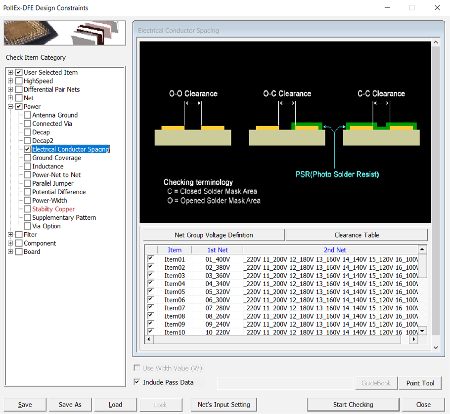
- Item: Input item name.
- 1st Net: The user presents the first net they want to verify.
- Net Group Voltage Definition: Here, the voltage value of the net can be set.
- Clearance Table: It is possible to specify clearance criteria based on the voltage range. Users can input values directly according to IPC specifications.
- 2nd Net: A list of all objects related to the first net and to be verified is automatically displayed. Here, Voltage difference (V) and clearance values for C-C, C-O, O-O are calculated and shown in the clearance table.
Through this feature, PCB manufacturers and designers can confidently produce circuits that meet rigorous spacing requirements by adhering to the standards set by the Institute for Printed Circuits (IPC). This ensures enhanced overall performance and durability of electronic devices, as they comply with stringent spacing demands.