Decap2
This rule checks a design guide for decoupling capacitor usage.
In order to stabilize a power supply, designers use de-coupling capacitors (by-pass capacitors). A fluctuation of power/ground affects component driving and results in bad signal transmitting. This Decap2 rule checks a design guide for decoupling capacitor usage. The usage guide for decoupling capacitors is that they should be placed within certain distance from a certain component’s power pin and connecting should be shorter than the given length. Long routing length between component power pin and decoupling capacitor cause an increase of inductance element and bad signal transmitting.
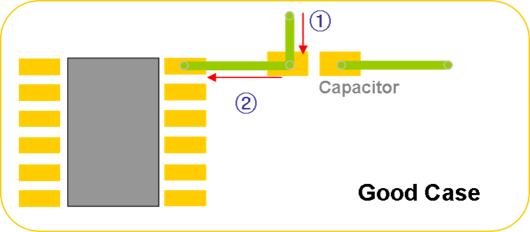
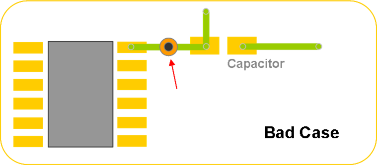
Recent design guides define all items described above. These new rule for using decoupling capacitor restrict the direct power connection to components. It is because when the power is assigned, decoupling capacitor will be charged first and then stable power would be supplied to the component power pin. The purpose of them is the components’ initial power stabilization. Also, for this purpose, avoid via between component power pin and decoupling capacitor. Shorter trace length is recommended.
-
Item: Input item name.
- Power Net: Select a power net group.
- GND Net: Select a ground net group.
- Decap Comp: Select a decoupling capacitor component group.
- Start Comp: Select a target IC net group that needs decoupling capacitors.
- Pin Type: Specify pin type for check. (Power Pin/GND/Power + GND)
- Power Pin: Check decap count of every power pin.
- GND Pin: Check decap count of every ground pin.
- Power + GND Pin: Check decap count of every power pin and ground pin.
- Ratio: Required ratio (Number of power pins which have decap/number of PWR pin)
- Distance: Assign a distance within which decoupling capacitors should be placed from IC components.
- Each Pin: Check decoupling capacitor existence per pin. The tool uses distance ⑧ to determine which decoupling capacitor belongs to which PWR/GND pin.
- Length: Assign required maximum trace length of decap. The capacitor which trace length is longer than this length will be excluded even though it is within the distance range ⑧.
- Each Pin (Length): Check decoupling capacitor existence per pin. The tool uses trace length⑩ to determine which decoupling capacitor belongs to which PWR/GND pin.
- Via: Checks if there exist via on trace between pin and decoupling capacitor.
- Branch: check if there exist branch on trace between pin and decoupling capacitor.
- Include Via Length: DFE will include via length for calculating trace length.
- Check Option
- Distance: Only decaps that exist within this distance from the power pin are considered valid decaps.
- Length: Only decaps whose routing length is shorter than this length from the power pin are considered valid decaps.
- Assign Decap one by one to each Power Pin: If this option is selected, decap sharing between power pins is not allowed.
- Check if VIA exists on the path: If this option is selected, it is judged as fail if VIA exists between the power pin and the decap.
- Check if Branch exists on the path: If this option is selected, it is judged as fail if Branch exists between the power pin and the decap.
- Include VIA Length: DFE will include via length for calculating trace length.
- VIA Length Compensation Factor: Effective length of VIA = VIA length * VIA length Compensation Factor.

Shorter lengths of ① and ② are better because they make small inductances.

- A key feature of DECAP is that the impedance is solely related to their loop inductance referred to as ESL (Equivalent Series Inductance).
- Decreasing the impedance of DECAP is all about decreasing the loop inductance of the complete path from the pin pads to the DECAP.
- The only way of decreasing the impedance of a DECAP at high frequency is by decreasing loop self-inductance.
- The best ways of decreasing the loop inductance of a DECAP are:
- Keep vias short by assigning the power and ground planes close to the surface.
- Use small-body-size capacitors.
- Use very short connections between DECAP pads and the vias to the underlying ground.
- Use multiple capacitors in parallel.
- Capacitors with good high frequency properties are often types of small capacity. Large capacitors usually have worse high frequency response.
Recommendations
- Use only one value of capacitor.
- Choose the capacitor based on the self-resonant characteristics from the manufacturers' data sheet to match the clock rate or expected noise frequency of the design.
- Use as many capacitors as needed for the range of frequencies to achieve the desired level of decoupling.
- Use a minimum of one capacitor per power pin, placed as physically close to the power pins of the IC as possible to reduce the parasitic inductance.
- Keep lead lengths on the capacitors below 6 mm between the capacitor endcaps and the ground or power pins.
- Place the bypass capacitors on the same side of the PCB as the ICs.