Placement
Analyze the location and orientation of a specified component on the board.
The placement of a component affects the quality of reflow and wave soldered assemblies. Proper soldering and placement prevents the adverse effects of stress on the component. For example, BGA-type components are weak on the diagonal areas of the board, so place them in a more suitable location.
More detailed information:
- Soldering Direction Definition: Input the soldering direction of the board.
Detect the soldering direction by analyzing the mark component or by
defining the direction manually.
- Component Group: Select a component group used for analyzing the
soldering direction and defining the library direction. The library
direction is the 0° direction of the mark component. For example,
the direction mark is registered as
 or 0° into the
footprint library, then placed in that fashion in the board. In this
case, the library direction is Left to Right. In some cases, the
direction mark is registered as or 0° into the
footprint library, then placed as
or 0° into the
footprint library, then placed in that fashion in the board. In this
case, the library direction is Left to Right. In some cases, the
direction mark is registered as or 0° into the
footprint library, then placed as  or 90°. In this
case, the library direction is Left to Bottom.
or 90°. In this
case, the library direction is Left to Bottom. - Soldering Direction: Input either horizontal or vertical as the soldering direction. After setting the soldering direction, define the placement direction of each component. Any component placed in a different way from the set direction is detected as an error.
- Table
- Item: Specify the item name.
- Component Group: Enter a component group for analysis.
- Placement: Input the component placement direction, also considered the soldering direction.
- Layer: Select a layer for analysis.
- Remainder: Select the component placement direction for the unspecified components on the board.
- Total Pass/Fail Ratio(%): Count the number of components passed per each selected group. If the calculated total ratio is less than the given ratio, an error is detected.
- Component Group: Select a component group used for analyzing the
soldering direction and defining the library direction. The library
direction is the 0° direction of the mark component. For example,
the direction mark is registered as
- Uniform Placement with Regular Interval and Straight Line: Input a component
group if specific components within the group must be placed on a straight
line with a regular interval.
Figure 1. Fail Type Example 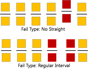
- Keep Component out of Board Center Area: Input specifications to avoid
component placement on the board center. Avoid the board center for
component placement due to the fragility during the soldering process and
the JIG fixture.
- Width: Input the width of the board center.
- Height: Input the height of the board center.
- Component Group: Enter a component group for analysis.
- Diagonal Placed BGA Check: Define the placement of a BGA-type component
after setting the soldering direction. Avoid placing BGA-type components on
the board center or corner.
- BGA Component Group: Enter a BGA component group for analysis.
Figure 2. Critical Area Width or Critical Area Ratio(%) 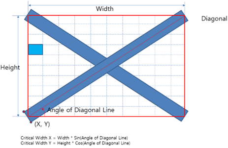
Figure 3. 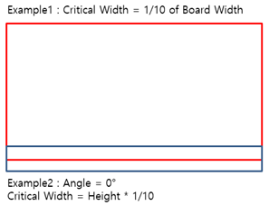
Figure 4. 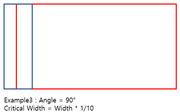
Figure 5. 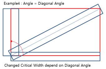
- Warpage Direction Definition: Enter the expected warpage direction
as diagonal or horizontal.
- Horizontal Axis Definition: Select the x-axis or y-axis for the horizontal case.
- Check only inside Component of Board Outline: Exclude components located outside of the board outline.
- Except for SMD pins, not having Metal Mask: Exclude components without metal masks from analysis.
- Placement Direction between Components: Analyze the placement
direction between components placed near each other. Define the base
component, peri-component, and the direction angle for use.
- Base Component: Select a base component for analysis.
- Base Component Distance: Define a distance from the base component for analysis.
- Expand Area: Enter a value for the expansion of the analysis area.
- Peri-component: Select a peri-component for the analysis or select All to check all the components.
- Placement Direction: Define the direction angle of the
peri-component.
Figure 6. Example 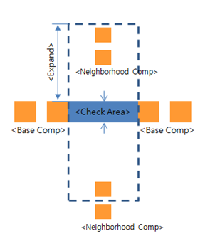
- BGA Component Group: Enter a BGA component group for analysis.
- Symmetric Placement Checking: Verify if a specific part is placed in
symmetry.
- Component Group: Enter a component group for analysis.
- Base Point of Symmetry: Select a base point for symmetry
analysis.
- Origin: Set the base point as the origin point in the design.
- Center: Set the base point as the center point of the board.
- Placement Prohibition Condition: Select locations on the board where
placement is prohibited.
- Item: Specify the item name for the result.
- Target Component Group: Select a specific component group or select
ALL to target all components for
analysis.
Figure 7. Component Group Select Dialog 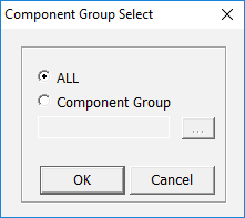
- Top/Bottom Layer: Enter a board layer for analysis.
- Use Component Group: Select a specific component group.Note: Recognize the keep-in/out area of the Use Component and check whether the Target Component is inside or outside
- Keep In/Out: Set the condition of the analysis to keeping the component in or keeping the component out of the analyzed board layers.
- Option: Set the conditions required for verification.
- Layer Existence: Verify the specified layers existence.
- Condition: Select to begin the analysis only if the specified component group is located on the analyzed layer.
- Tolerance: Set the tolerance for the component placement analysis on the selected layer.
- Except Area: Enter an area to exclude from the layer analysis.