BUS is a bundle of signals that have the same signal attributes.
DATA and ADDRESS lines are examples of BUS. In order to keep the same signal
attributes, they have the same length, width and via.
Note: In
case of source synchronous technology, send the clock (strobe) signal to be used
to capture data with the data signal.
This item checks the following:
The delay time between bus nets.
The delay time between bus nets and strobe signal.
The timing skew between differential pair nets.
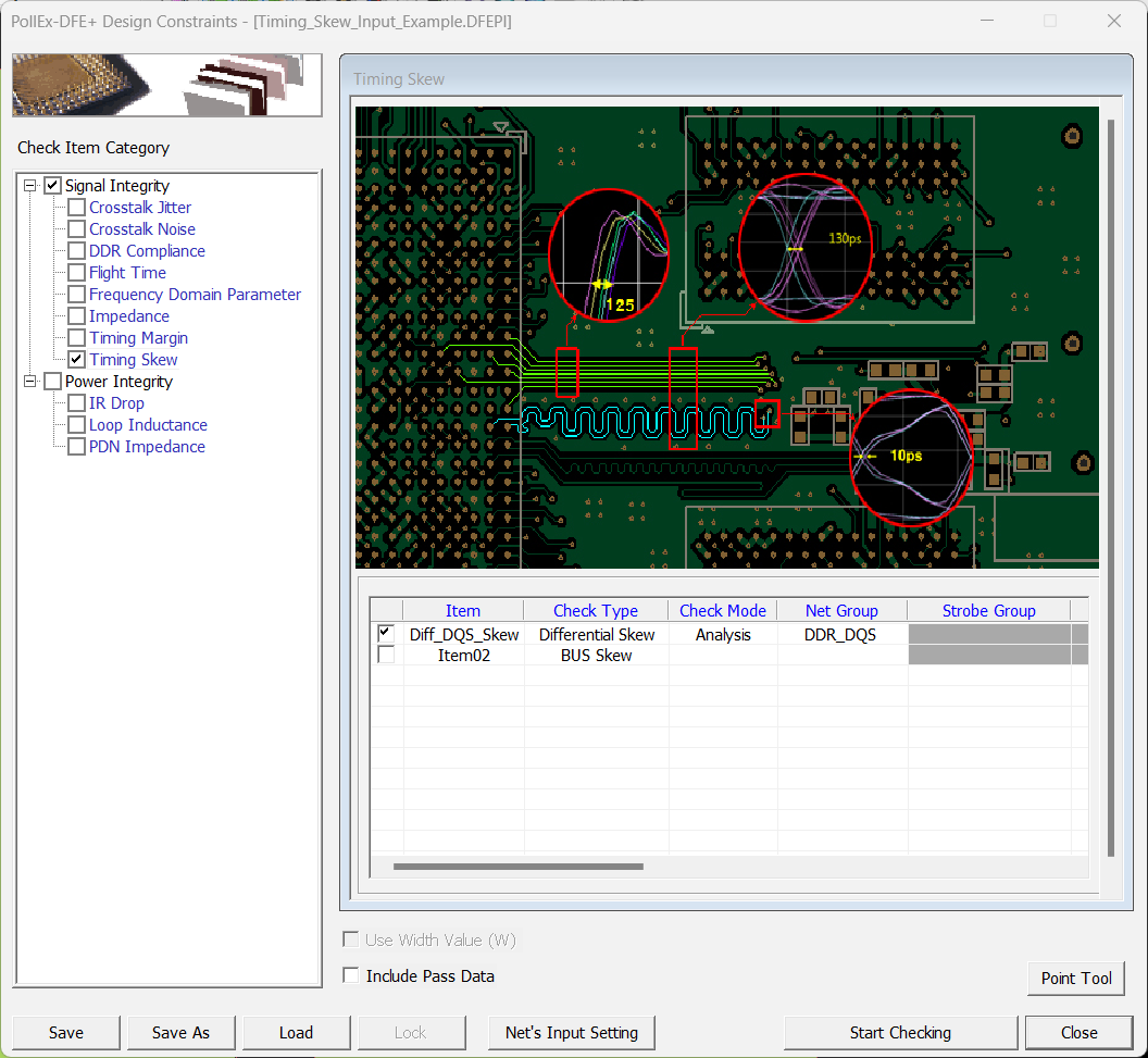
Figure 1.
Item: Sub item name. You can enter arbitrary name.
Check Type: Select a check type.
BUS Skew: Check the delay time difference between bus nets.
Strobed BUS Skew: Check the delay time difference between bus nets
and strobe signal.
Differential Skew: Check the delay time difference between the
positive (+) and negative (-) signal with single differential
pair.
Strobe to Strobe Skew: Check the delay time difference between
strobe nets.
Differential Inter-pair Skew: Check the delay time difference
between multiple differential pair nets.
Check Mode:
Analysis: Check skew performing waveform and eye-diagram analysis to
check for skew.
TML: Check skew using Transmission Line Analysis results and the VIA
delay formula.
Net Group: Select target net groups to be tested. Allow multiple net
groups.
Strobe Group: Option to select target strobe net groups to be tested (Clock,
DQS, and so on).
Net Combination: Option to establish correlation between Strobe Net and
Dependent Net.
Start Component: Select component group to be used as signal driver.
Except Component: Select component group to be excluded. Allow multiple
component groups.
Analysis Mode:
Common mode: This is the part of the signal that appears equally on
both lines of a differential pair. Common mode can result from
external interference or imbalances and doesn’t contribute to the
intended data signal.
Differential mode: This is the actual difference in signal between
the two lines in a differential pair, which carries the intended
data.
Period(nS): Enter operating period in nS unit.
Skew(pS): Enter allowable maximum skew in pS unit.
Tolerance(%) option: Enter allowable tolerance of skew.
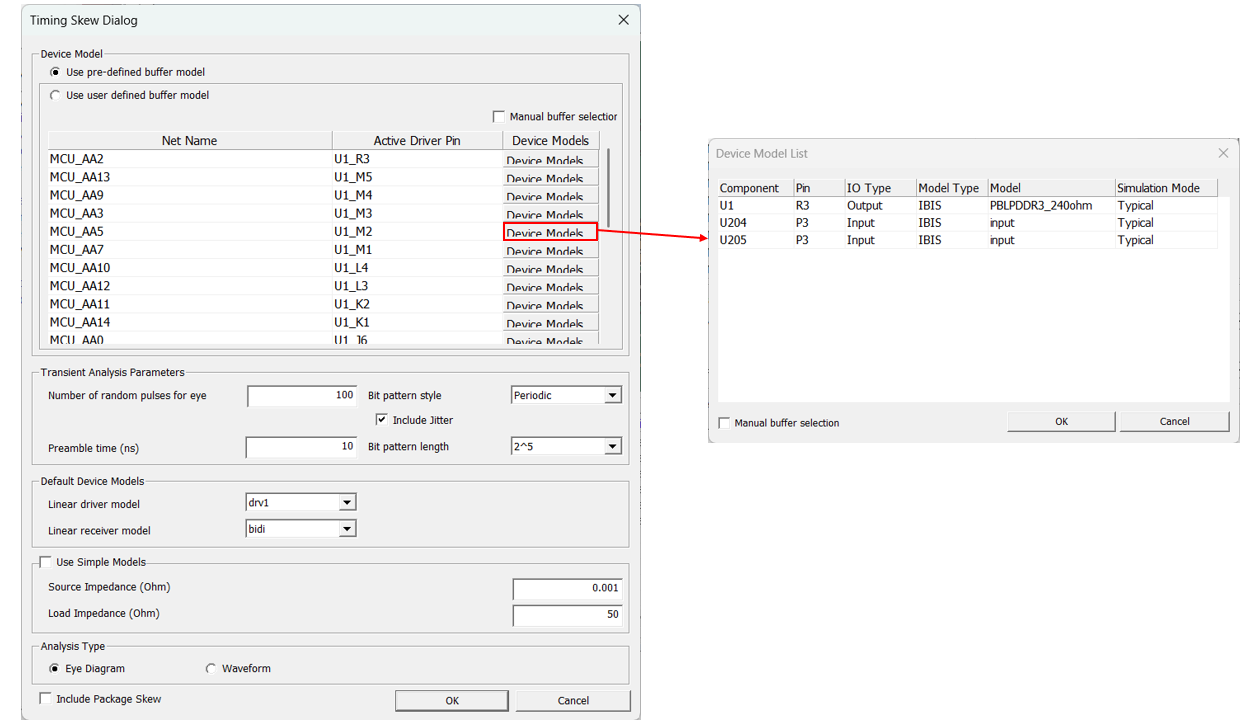
Analyze Options: You can assign driver/receiver buffer simulation model,
driving strength of driver and other simulation parameters.
There are two ways to assign the simulation buffer model:
Use pre-defined buffer model: The buffer model set in the electrical pin
part of UPE is used as default. You cannot change the buffer model
here.
Use user defined buffer model: You can assign simulation buffer model.
The default buffer model is initially assigned to the buffer model field which can be
changed.
Clicking Model field allows you to view the device models
selected for the output and input pins. You can change the device model selection
when multiple models are available for the pin.Figure 2.
Prior to running analysis, you can change the analysis control parameters such as the
number of random pulses and bit pattern style.
Model: The default buffer model is initially assigned
to the buffer model field which can be changed by users. For the selected
active driver, actual driver model can be selectable among many different
models in IBIS or Linear device model types. You can use one of available
models considering the output impedance, driving capability measured by
output current level and operating frequencies. These driver’s
characteristics lead huge impact on the simulated waveforms.
Simulation Type: You can select the simulation type
also among Typical, Fast, and Slow. The simulation type is applied to all
device models used for the analysis.
Number of random pulses for eye diagram: Means the
number of random pulses excited to the simulating net during the eye diagram
analysis.
Preamble time: Simulation start after this time to wait
until status of internal circuit becomes stable.
Bit pattern style: Select the numerical method among
random, ABS (Artificial Bit Stream) and PRBS (Pseudo Random Bit Stream) for
generating the bit sequences. ABS (Artificial Bit Stream) is a method
designed to provide a large pattern of bits to show worst case signal
transmission quality of the net that would quickly converge the eye diagram.
PRBS (Pseudo Random Bit Stream) is the mostly common method deemed as an
industry standard.
Bit pattern length: If bit pattern style is ABS or
PRBS, choose the bit pattern length here.
Default Device Models: When the device models are not
available in the part data, the default device models defined here are used
for transient simulation of signal integrity analyses. With the use of
Linear Device Modeler, users can create linear output (driver) and input
(receiver) device models and store them in a linear device model file.
PollEx DFE+ provides users with a system default linear device model file,
UDVS.dmf.
Use Simple Models: This function allows users to
specify source impedance and load impedance when measuring timing skew.
Analysis Type: Choose between eye diagram and waveform
analysis.
Include Package Skew: Measure the Skew by considering
the Package Delay of the parts. Package delay can be set through the Package
Length Parameter tab for each part in the Properties-Parts menu.
Important: The following are the
Unsupported Stackup Cases for Timing Skew:
Presence of a Floating Layer
If a Floating Layer exists at any level within the
stackup structure, the Timing Skew Analysis
will fail.
Coating Layer Included in Inner Layers
If a Coating Layer is placed within the
Inner Layers, the analysis will result in
failure.
Consecutive Dielectric Layers
If the stackup contains continuous Dielectric
Layers, the analysis will fail.
Consecutive Signal Layers
If there are continuous Signal Layers in the
stackup, the analysis will fail.
Remember: If there are unsupported
structure, the result comes out as failed.