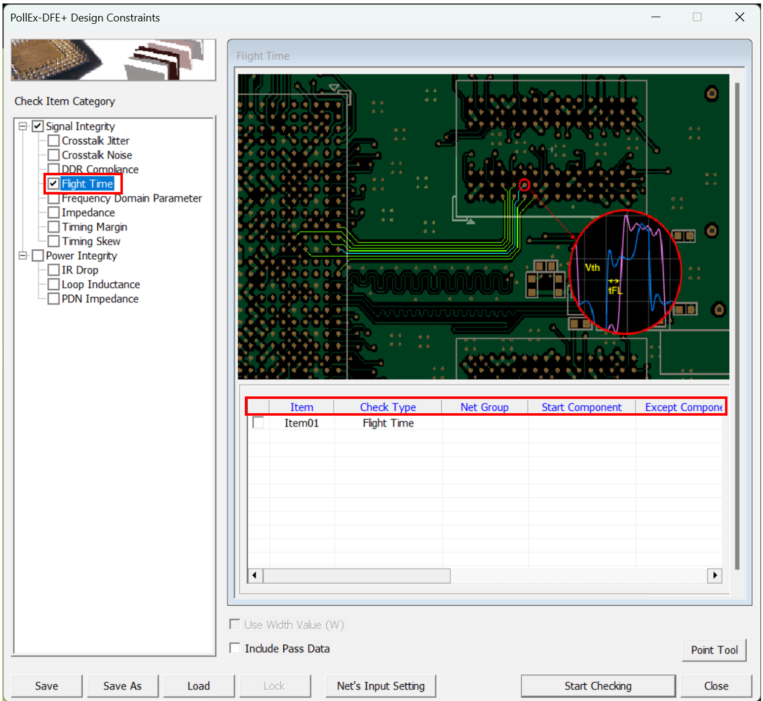
Flight Time
This item checks the propagation time from the driver to the receiver, where the signal is transmitted.
- The time it takes for the signal to pass from the driver to the receiver.
- Two types of measurement standard - Pin to Pin, Die to Die.
- Flight time is used interchangeably with propagation delay.
- It used to limit the trace length considering losses.

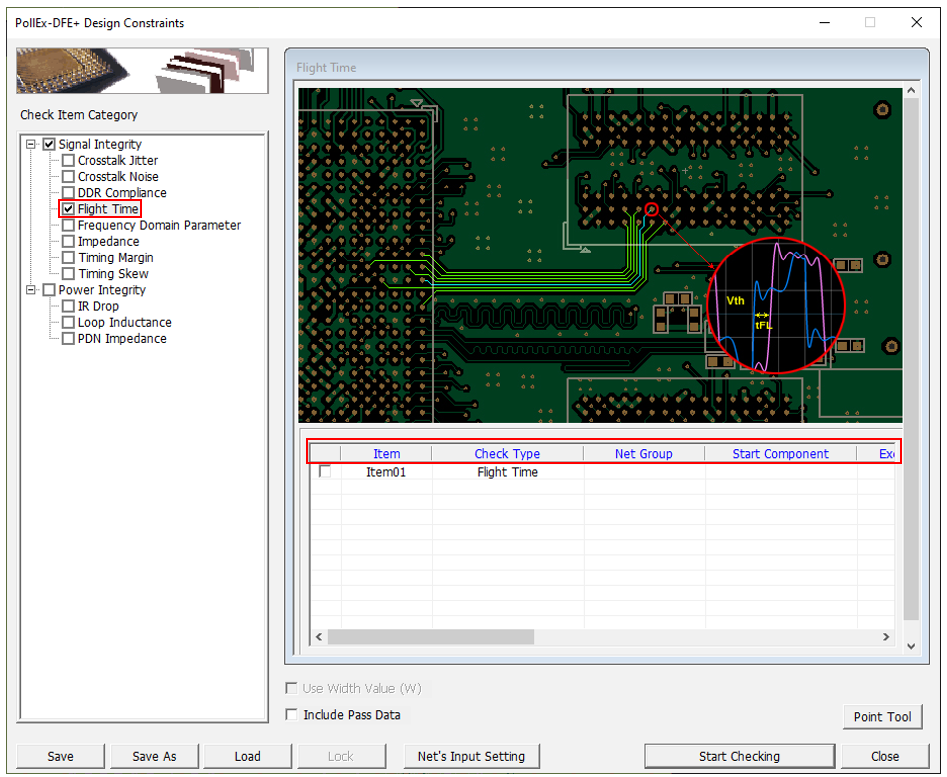
- Item: Enter sub item name. User can enter arbitrary name.
- Check Type: Select Flight Time analyze method.
-
Flight Time: Using the Waveform Analysis feature, measure the Flight Time taken for the Signal to reach the Receiver from the Driver
-
Delay Time: Utilizing the Transmission Line Analysis feature, calculate the total delay time of the net.
-
-
Net Group: Select target net groups to be tested. Allow multiple net groups.
- Start Component: Select the component to drive the signal.
- Except Component: Select components that should be excluded when measuring Flight Time.
- Frequency (MHz)
- Vth: The reference voltage used as a basis for measuring Flight Time.
Figure 2. 
- Use default voltage from simulation model: Use the reference voltage defined in the simulation model.
- Use user defined voltage(V): The user inputs the reference voltage directly.
- Flight/Delay Time(pS): Required Flight/Delay Time in pS
- Tolerance(%)options: Enter allowable tolerance of Flight/Delay Time.
- Analyze Options: You can assign driver/receiver buffer simulation model, driving strength of driver and other simulation parameters.
-
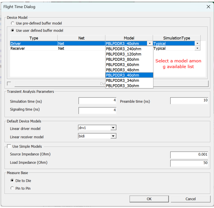
There are two ways to assign the simulation buffer model:
- Use pre-defined buffer model: The buffer model set in the electrical pin part of UPE is used as default. You cannot change the buffer model here.
- Use user defined buffer model: You can assign simulation buffer model.
-
The default buffer model is initially assigned to the buffer model field which can be changed.
Clicking Model field allows you to view the device models selected for the output and input pins. You can change the device model selection when multiple models are available for the pin.
Figure 3. 
- Prior to running analysis, you can change the analysis control parameters
such as the Simulation time, Signaling time and Preamble time.
- Model: The default buffer model is initially assigned to the buffer model field which can be changed by users. For the selected active driver, actual driver model can be selectable among many different models in IBIS or Linear device model types. You can use one of available models considering the output impedance, driving capability measured by output current level and operating frequencies. These driver’s characteristics lead huge impact on the simulated waveforms.
- Simulation Type: You can select the simulation type also among Typical, Fast, and Slow. The simulation type is applied to all device models used for the analysis.
- Simulation Time(ns): Enter end time of the SPICE transient analysis.
- Signaling Time(ns): Input Signal having pulse period will be excited to the net until the time assigned here.
- Preamble time: Simulation start after this time to wait until status of internal circuit becomes stable.
- Default Device Models: When the device models are not available in
the part data, the default device models defined here are used for
transient simulation of signal integrity analyses. With the use of
Linear Device Modeler, users can create linear output (driver) and
input (receiver) device models and store them in a linear device
model file. PollEx DFE+ provides users with a system default linear
device model file,
UDVS.dmf. - Measure Base: Setup the Flight Time measure base.
- Die to Die: Measure the time taken for the signal to reach from the Driver Die to the Receiver Die when measuring Flight Time.
- Pin to Pin: Measure the time taken for the signal to reach from the Driver Pin to the Receiver Pin when measuring Flight Time.