Approach Prohibition Via
This item checks for high speed signal’s inner via structure.
In many cases, designers use inner layer vias to get routing space on a board. If
inner vias are used for highspeed signal trace, they may cause a problem when common
signal traces are routed above or below the inner via. High speed signals via can
give bad influence to common signal. This structure results in small crosstalk, but
if the signal is in quite status and connected to outside of board, common signal
could be activated as antenna. And this structure causes EMI problems.
- Exclude Net: Select exception nets to exclude vias that stabilize signal such as ground via.
- Item: Input item name.
- Net: Select High Speed Signal Net Group.
- Clearance: Set a clearance between assigned net/via and vias in other nets.
- Check Layer: Set a layer for via clearance checking.
-
- The PollEx DFE report will show detected nets with their clearance from via.
- All Layers: check all layers.
- L1 Layer: check one layer above and below.
- L2 Layer: check two layers above and below.
- Component Keep IN/OUT: You can define the test region with this option. For
example, you can test inside or outside the breakout region of CPU with
different test value.
- Component Group: Select required component group which is used for defining the test region.
- Range (COC+distance): Enter the distance value to define breakout range. The COC (Component Overlap Check) plus this distance value is considered the test range.
- Region: Define the required test region.
IN: Test inside of the breakout region of target component.
OUT: Test outside of the breakout region of target component.
- Target Layer: Select the required test layer.
- All Layer: Test all layers.
- Component Place Layer: Test only component placement layer.
- Different Rule Setup in Special Region: Assign additional test
region for breakout region testing.
- Extended Region from COC: Enter the distance value to define additional range. The COC (Component Overlap Check) plus this distance value is considered the additional test range.
- Allowable Values: Assign additional allowable test value for
this additional region.
- Value: Add additional allowable value.
- Range: Add additional allowable range.
- Deviation: Add additional allowable value with deviation using this option.
- Deviation (%): Add additional allowable value with deviation (%)
- Not check between nets in same group: Separation between same net group signals will not be checked.
- Pin Escape: Enter a radius of circular region around pins to be excluded for
the rule check.
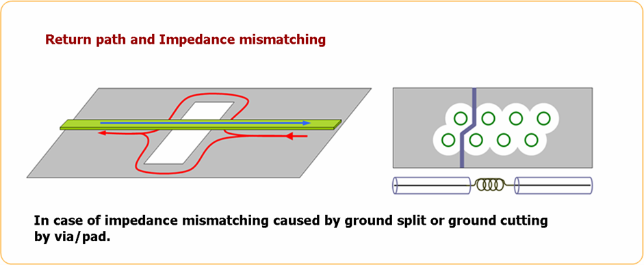
Since BB vias cannot be easily visible and placed in inner PCB layers, they may be placed under a high-speed signal and may generate noise by impedance mismatching. Because of such reason, designers should be careful while placing BB vias.
BB Via: Buried Via, Blind ViaFigure 1. 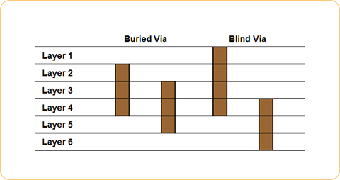
Figure 2.