Zuken CR5000 PWS
PollEx PCB supports two types of reading: artwork and wiring modes for Zuken PWS. Artwork mode means that all objects in design have no intelligent information like net name. All routing patterns exist on physical layers, but they don’t have net information, so they will be transferred to just graphic data. In this case, after reading design with artwork mode, user cannot use these designs for nets related function or for electrical analysis.
| File | |
|---|---|
| *.BSF | Board specification information file |
| *.CCF | Net information file |
| *.MDF | Part information file |
| *.UDF | Component placement and board graphic information file |
| *.WDF | Routing pattern information file |
- Extract ASCII file from Zuken CR5000 PWS.
-
From the menu bar, click .
The Import from Zuken PWS dialog opens.
- Layer Setup: Use this setting to read layer definitions into PollEx PCB design. Zuken PWS designs may have different layer settings depending on users and depending on manufacturing process. To complete this task, refer the BSF (Board Specification File) file used in PWS.
- Board Contour Layer: Specify the board contour layer number, in case of using board contour layer differently than that is used in BSF.
- Exclude Layers: Exclude specified layers.
- Load ZLS File: Import a Zuken PWS layer setting file (*.zls).
- Save As File: Save a Zuken PWS layer setting file (*.zls).
- Apply to Environment Setting: Apply settings to the environment setting.
- PWS ASCII File(*bsf): Select the target ASCII file *.bsf to import.
Figure 1. 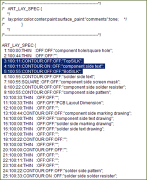
To define usage of artwork layers in PWS, it is preferred to define all top/bottom corresponding layers. These layers mapping status can be saved into file, *.zls, and re-use it for the next reading.