Use PollEx Logic to review schematic design. You can check
symbols and nets in sheets.
PollEx Logic DFE is a toolset which can check electrical
validity and standardizing of schematic design. PollEx Logic DFE is an option module of PollEx Logic and it helps designers to reduce recursive design
errors that might be detected in the post design processes. Using standard net names
in Schematic makes PCB CAD work much easier. You can use PollEx Logic DFE to set a standard net naming convention. The
results of PollEx Logic DFE can be exported in an MS/Excel
spreadsheet.
The tutorial related files are provided by default after installing PollEx at the following path:
C:\ProgramData\altair\PollEx\<version>\Examples\Verification\LDFE
Open and Preview Schematic Design
In this step, you will open a design file and preview the schematic
design.
Start PollEx Logic.
From the menu bar, click File > Import CAD > SDB Binary.
Open the
PollEx_Logic_sample_r<revision_number.sdbb
file from
C:\ProgramData\altair\PollEx\<version>\Examples\PollEx_Logic_sample_r<revision_number>.sdbb.
<Version> means the version of PollEx that you are currently
using.
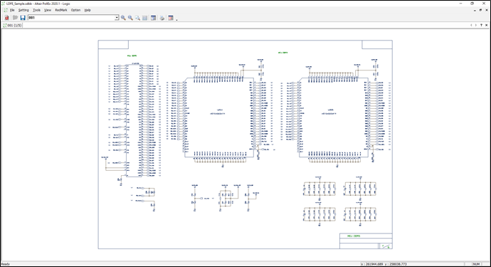
The LDFE_Sample schematic is displayed as shown below.Figure 1.
From the menu bar, click Tools > Schematic Data Extractor to preview schematic design and see information about Components
and Nets.
To setup Logic DFE input, you must review the current design. The sample
design consists of CPU and two DDR3 memories.
Check Connected Comp
In this step, you will launch Logic DFE and check the connected comp.
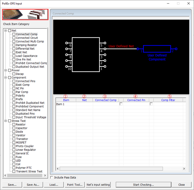
From the menu bar, click Verification > DFE > Input.
The PollEx DFE Input dialog opens.Figure 2.
Preview Connected Comp item. Normally, the easiest way to generate a reference
voltage is to use Voltage Divide Logic using resistor network.
In this case, the resistor should have 1% tolerance to ensure the accuracy of
the output voltage value. You can check this requirement using the Connected
Comp item.
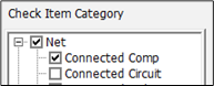
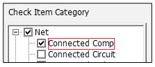
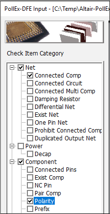
In the Check Item Category section, enable the Connected
Comp checkbox.
Figure 3.
The Connected Comp Item Rule Entry dialog
opens in the Input dialog.
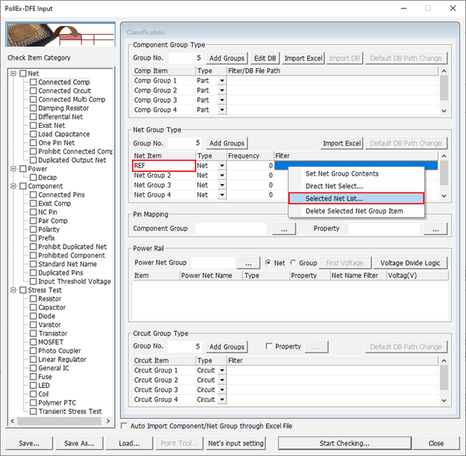
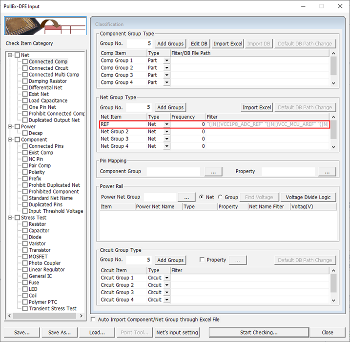
Define net groups.
In the PollEx-DFE Input dialog, click the
classification menu.
Figure 4.
The PollEx-DFE Input dialog
opens.
Define REF net group.
In the Net Group Type section, double-click Net Group
1 and change the group name to
REF.
From the Net Name list, select REF.
From the Filter tab, right-click and select Select Net
List from the context menu.
Figure 5.
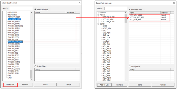
Select Selected Net List.
Select the following nets from the net list:
VCC_MCU_AREF,
VCC_DDR_REF, and
VCC1P8_ADC_REF.
Click Add to List.
Figure 6.
Click Done.
The selected list will register as net group, REF.Figure 7.
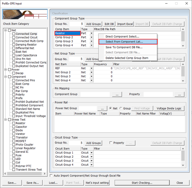
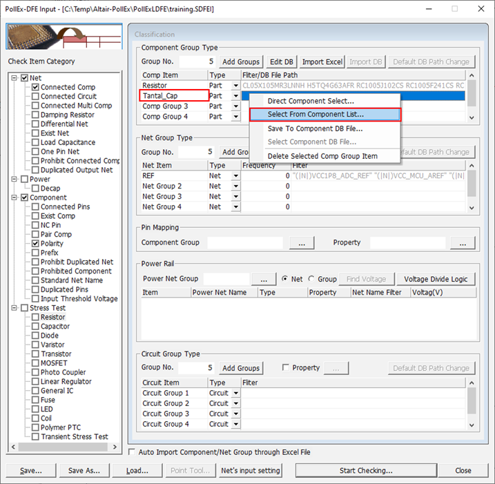
Define Resistor component group.
In the Component Group Type section, double click Component
Group 1 and change the group name to
Resistor.
From the Comp Name list, select Resistor.
From the Filter/DB File Path tab, right-click and select
Select From Component List from the context menu.
Figure 8.
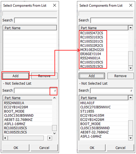
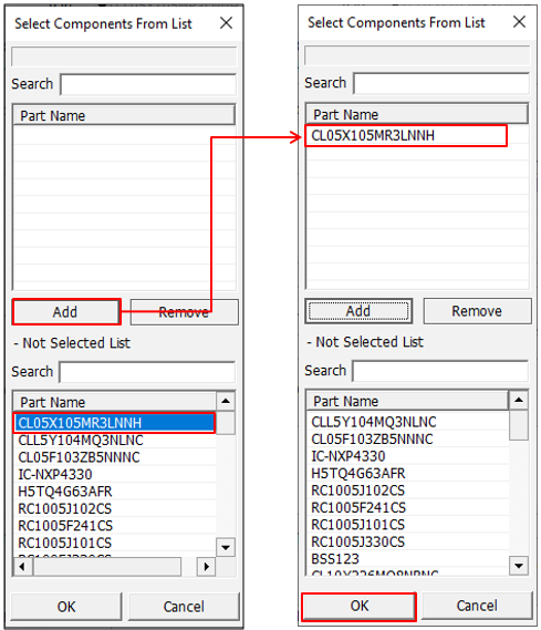
Select Selected Component from List.
In the Search field, enter R and click
Add.
Figure 9.
Click OK to close
this window.
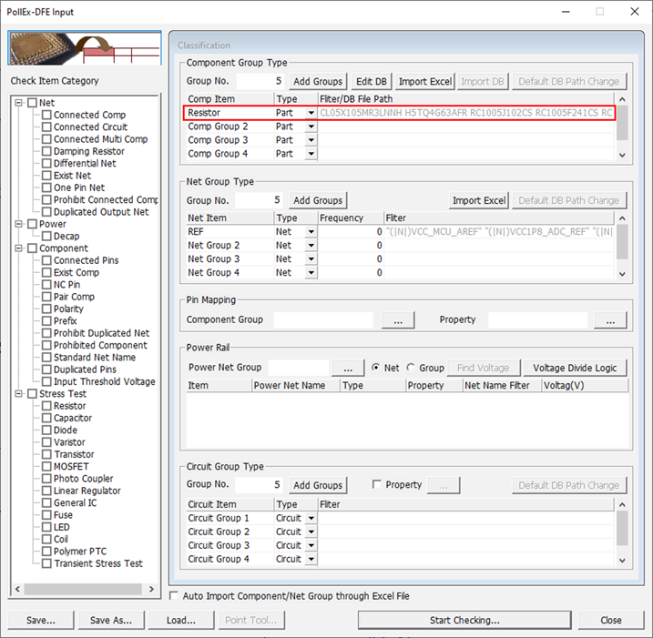
The selected list is registered as a component group with name,
Resistor.Figure 10.
Set Connected Comp item test condition.
Click Connected Comp item.
The Connected Comp Item Rule Entry dialog opens
in the PollEx Logic DFE Input dialog.Figure 11. Figure 12.
Double-click the Net field of the first
item.
The Select Group dialog opens.
Select the REF net group and click
OK.
Double-click the Item field of the first item
and enter Vref_Resistor_Tolerance for the name of
the sub-item.
Double-click the Connected Comp field of the
first item.
The Select Group dialog opens.
In the Select Group dialog, select the
Resistor component group and click
OK.
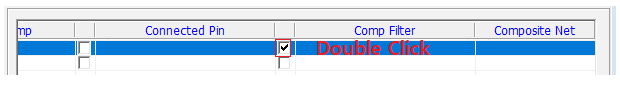
Enable the Comp Filter checkbox and double-click
the Comp Filter field of first item.
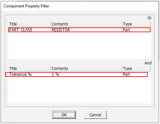
The Component Property Filter dialog
opens.Figure 13.
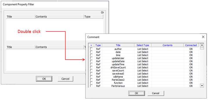
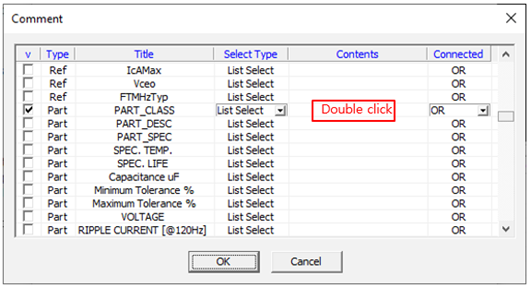
Double-click the empty field.
The Comment dialog opens.Figure 14.
Select Part_CLASS from the drop-down list of the
Title column and enable the checkbox.
In the Select Type column, select List
Select.
In the Connected column, select OR.
Figure 15.
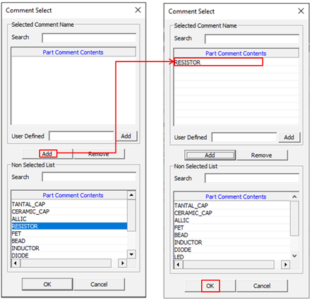
Double-click the field in the Contents
column.
The Comment Select dialog
opens.
Under Part Comment Contents, select RESISTOR and
click Add.
Figure 16.
Click OK to close
Comment Select dialog.
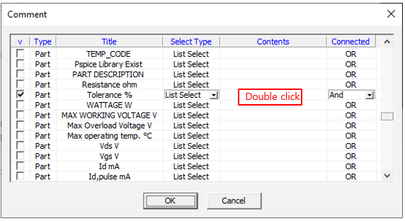
In the Comment dialog, enable the
Tolerance % checkbox.
For Select Type, select List Select.
For Connected, select And.
Figure 17.
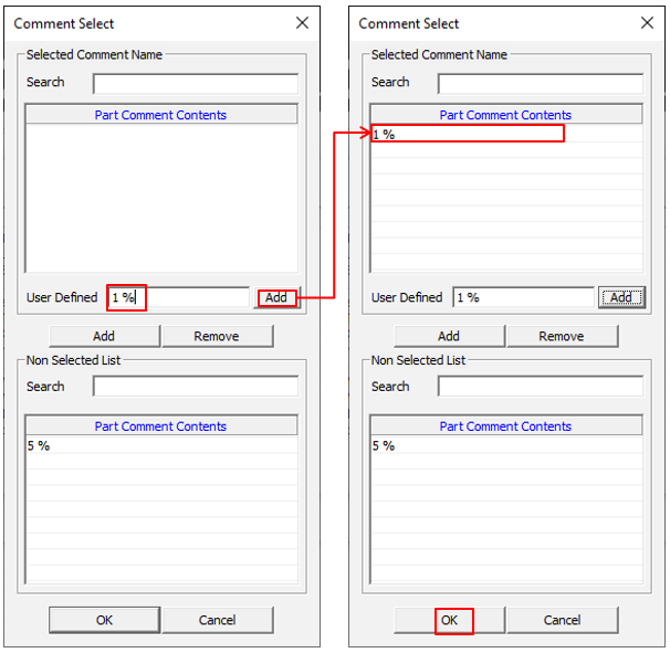
Double-click the Contents field.
The Comment Select dialog
opens.
In the Comment Select dialog, enter
1% string in the User Defined field and click
Add.
Figure 18.
Click OK to close the
Comment dialog.
In the Component Property Filter dialog,
the new PART_CLASS property is added in the OR section. Tolerance % is
added in the AND section of the Component Property
Filter dialog.Figure 19.
Click OK to close the
Component Property Filter dialog.
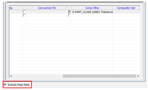
Enable the Include Pass Data checkbox.
Figure 20. With this setting, PollEx Logic DFE
checks if a 1% tolerance resistor is connected to the voltage divide
logic for REF signal group.
Run Connected Comp Item and review Check Result.
Click Save As and save the input file as
training.SDFEI in the
PollExLDFE folder under job folder.
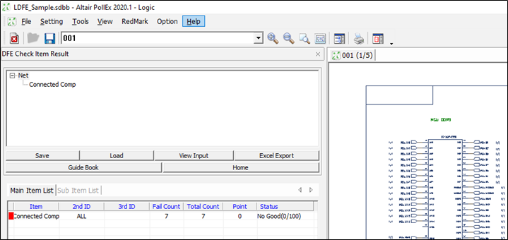
Click Start Checking.
PollEx Logic DFE begins checking for
selected checking items. After running, the results display.Figure 21.
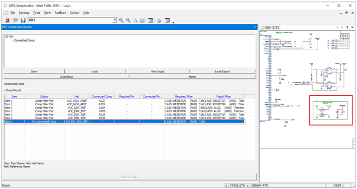
In the result tab, click Connected Comp in the
Item column.
The detail error list displays.
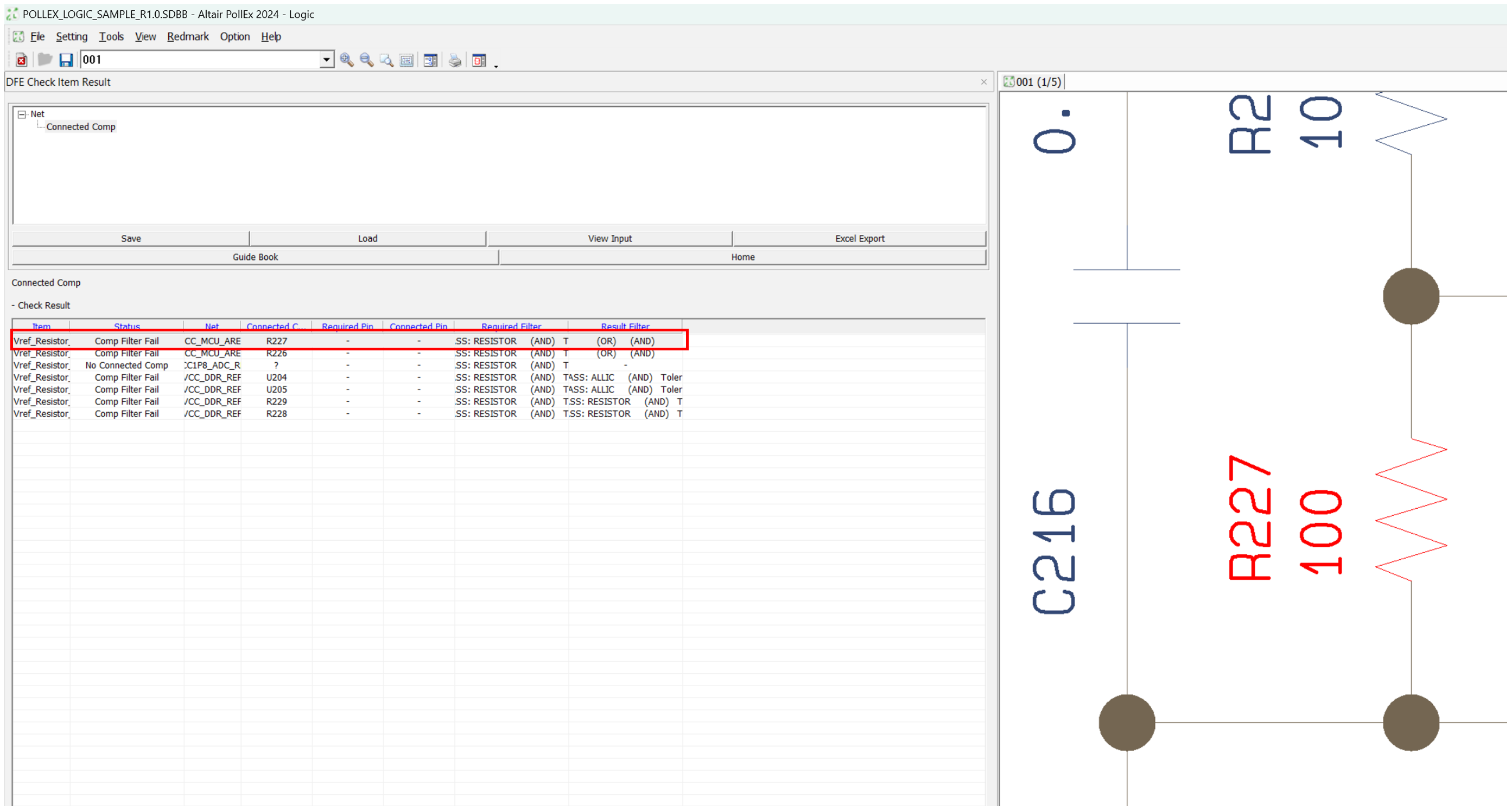
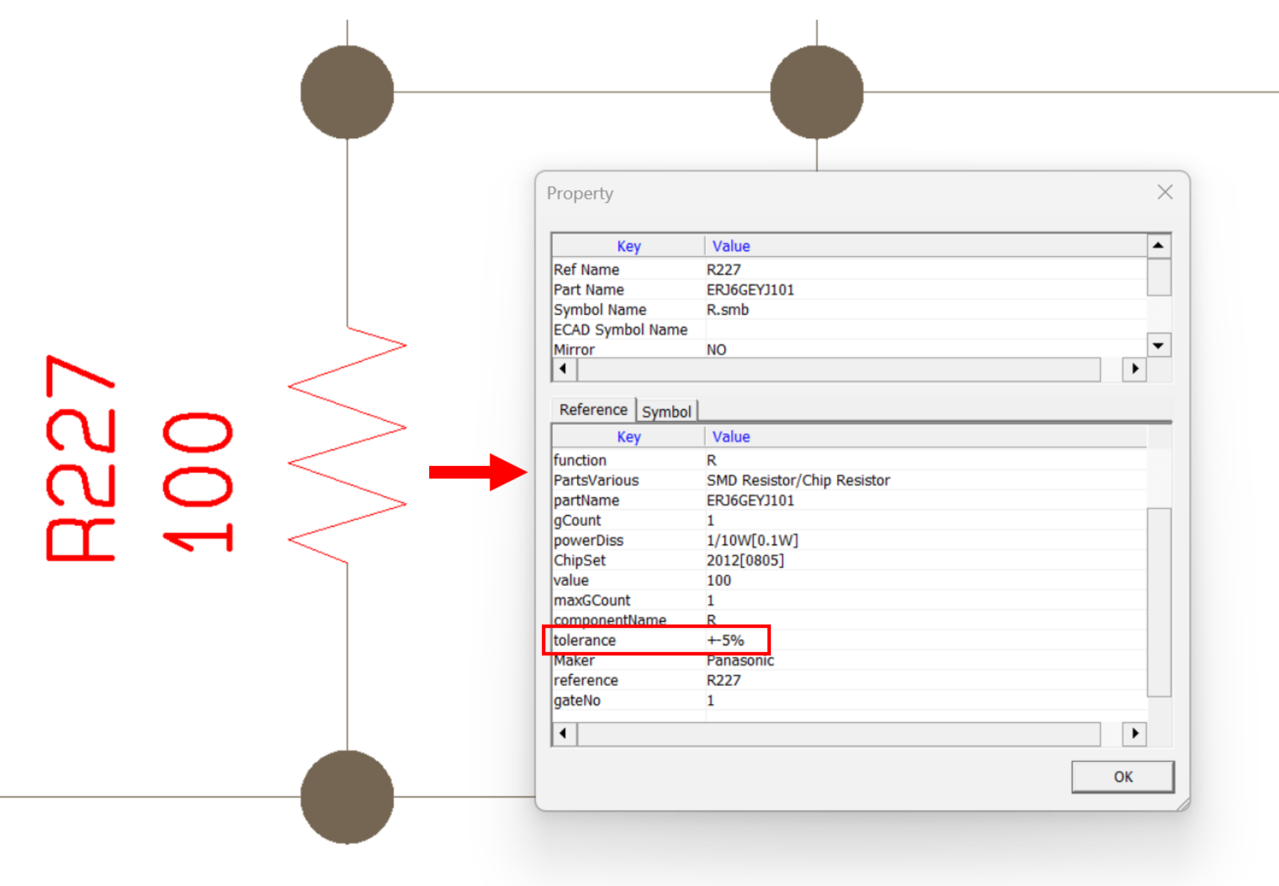
Click the error item R227 in the Connected Comp
field.
Figure 22.
Select R227, right-click and select
Select Property from the context menu.
The Property dialog opens.
In the Symbol tab of the Property dialog, review
the property of the R227 component.
The R227 component should have a 1% tolerance, but with a 5% tolerance
the result is failed.
Click OK to close the
Property dialog.
Figure 23.
In the result tab, click the No Connected Comp
error item.
There is no resistor connected to VCC1P8_ADC_REF net, so the result is
failed.Figure 24.
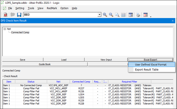
Generate Excel Report
In this step, you will generate an Excel report for the result.
In the result tab, click Excel Export and select
User Defined Excel Format.
Figure 25.
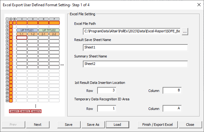
The User Defined Export Excel dialog
opens.
Excel file setting.
Click Load and open the training.SDFEE file from
C:\ProgramData\altair\PollEx\<version>\Examples\Verification\LDFE\SDFEE.
Accept the other default parameters.
In the User Defined Export Excel dialog, your
settings should now look as follows:Figure 26.
Click Next.
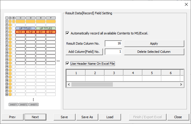
Result Data [Record] field setting.
Enable the Automatically record all available Contents to
MS/Excel checkbox.
For Result Data Column No., enter 16 and click
Apply to extend the column count to 16.
The LDFE provides a total of 16 kinds of information.
Enable the User Header Name On Excel File
checkbox.
Figure 27.
Click Next.
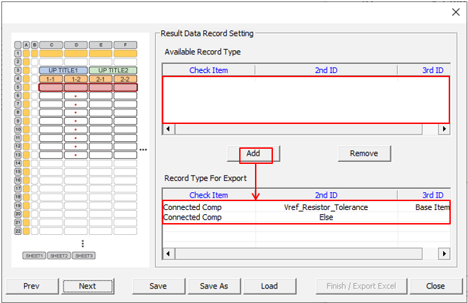
Result Data Record setting.
The upper section shows total available result items. And the lower section
shows selected item for excel report. You can manually select the items to be
included in the excel report by clicking Add. Enable the
Automatically record all available Contents to
MS/Excel checkbox to automatically select all items.Figure 28.
Click Next.
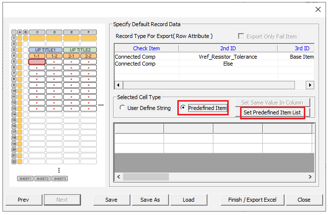
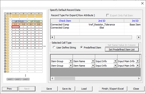
Specify Default Record Data.
Select Predefined Item and click Set
Predefined Item List.
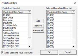
The Predefined Item dialog opens.Figure 29. Figure 30.
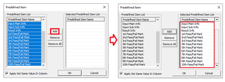
Click Remove All.
Select all items available in the left section of the dialog except
first item named [BLANK] and click Add.
Select Apply Set Same Value in Column.
Your settings should now look as follows:Figure 31.
Click OK.
Figure 32.
Click Save As and save this report setup
environment file as training.SDFEE in the
PollExLDFE folder under the job folder.
Click Finish/Export Excel to start Excel report
creation.
PollEx Logic DFE begins generating
excel report. After running, PollEx Logic DFE
shows the excel report file.
Save this Excel file.
Check Polarity
Polarity check
In the result tab, click View Input.
The PollEx-LDFE Input dialog
opens.
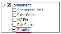
Enable the Component and
Polarity checkboxes.
The Polarity item rule entry dialog
opens.Figure 33.
In the PollEx-DFE Input dialog, click the classification
menu above the Check Item Category section.
Figure 34.
The PollEx-DFE Input dialog opens.
Define Tantal_Cap component group.
In the Component Group Type section, double click Component
Group 2 and change the group name to
Tantal_Cap.
Right-click in the Filter/DB File Path field and
select Select From Component List.
Figure 35.
Select the CL05X105MR3LNHN component from part
name list in lower section and click ADD.
Figure 36.
Click OK.
The selected list is registered as component group Tantal_Cap.
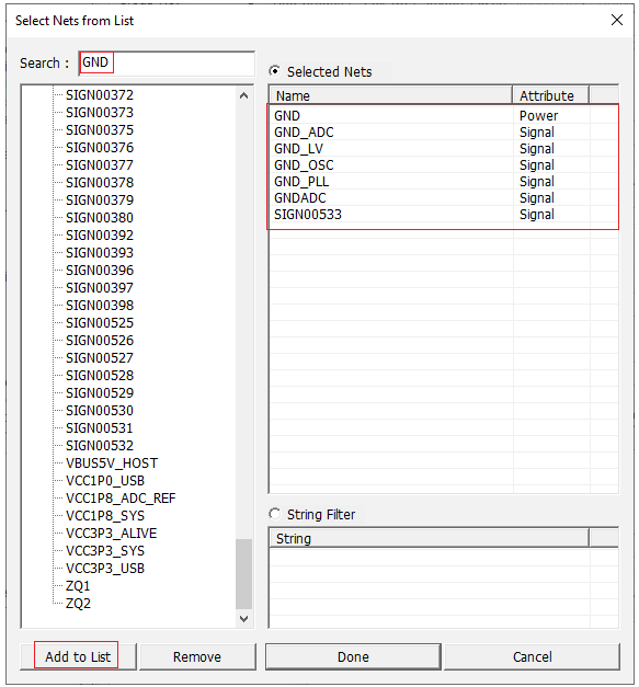
Define Ground net group.
In the Net Group Type section, double click Net Group
2 and change the group name to
Ground.
Right-click in the Filter/DB File Path field and
select Select Nets List.
The Select Nets from List dialog
opens.
In the Select Nets from List dialog, enter
GND in the Search field.
Click Add to List.
Figure 37.
Click Done.
The selected list is registered as net group Ground.
Enable the Polarity checkbox in the Check Item
Category list.
Figure 38.
The Polarity Item Rule Entry dialog
opens.
Set Polarity item test condition.
Figure 39.
In the Polarity Item Rule Entry dialog,
double-click the Net field.
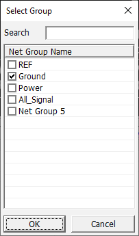
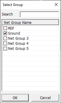
The Select Group dialog opens.Figure 40.
Enable the Ground checkbox and click
OK.
In the Polarity Item Rule Entry dialog,
double-click the Item field and enter
Tantal_Polarity_Check for the sub-item
name.
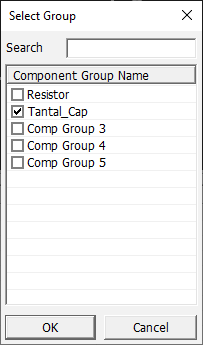
Double-click the Comp field in the
Polarity Input Setup dialog.
The Select Group dialog opens.
In the Select Group dialog, enable the
Tantal_Cap checkbox and click
OK.
Figure 41.
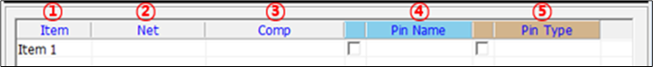
Choose the Pin Name.
Figure 42.
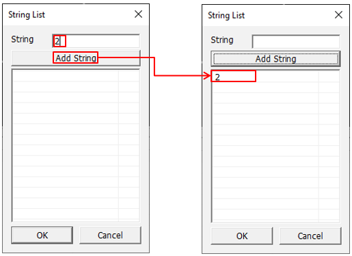
Double-click the Pin Name field in the
Polarity Input Setup dialog.
The String List dialog opens.
In the String List dialog, enter
2 for String and click Add
String.
Click OK to close the
String List dialog.
Figure 43.
Click Save to save the current setup.
Run Polarity Item and review Check Result.
Click Start Checking.
PollEx Logic DFE starts checking for
selected checking items. After running, the results
display.
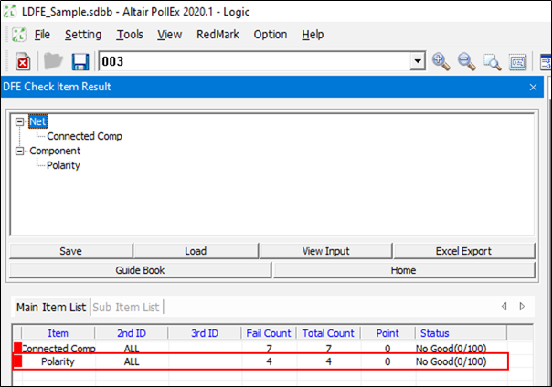
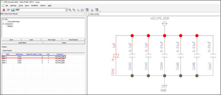
In the result tab, click Polarity to see the
detailed result.
Figure 44.
In the result tab, click C241 in the Reference
field.
The positive pin of C241 is incorrectly connected to the ground, so it
has failed.Figure 45.
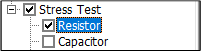
Check Stress Test
In the Result tab, click View Input.
The PollEx-DFE Input dialog opens.
Enable the Stress Test and
Resistor checkboxes.
The Stress Test/Resistor Item Rule Entry dialog
opens.Figure 46.
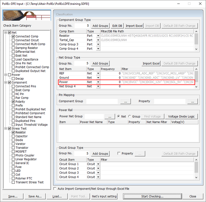
Define Power net group.
Click the classification button menu.
Figure 47.
The PollEx-DFE Input dialog
opens.
In the Net Group Type section, double-click Net Group
3 and change the group name to
Power.
Right-click the same line and select Selected Net
List from the context menu.
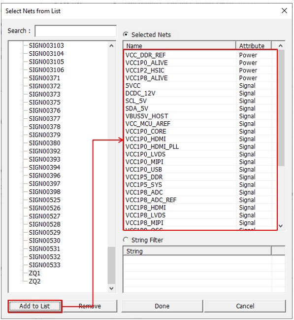
Select the following power nets: 5VCC,
DCDC_12V, SCL_5V,
SDA_5V and all other nets whose name is begin
with VCC string.
Click Add to List and click
Done.
Figure 48. The selected list is registered as the Power net group.Figure 49.
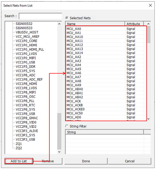
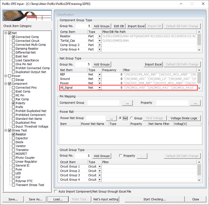
Define All_Signal net group.
In the Net Group Type section, double-click Net Group
4 and change the group name to
All_Signal.
Right-click the same line and select Selected Net
List from the context menu.
Select all signal nets except all power and ground nets.
Click Add to List and click
Done.
Figure 50.
The selected list is registered as All_Signal.Figure 51.
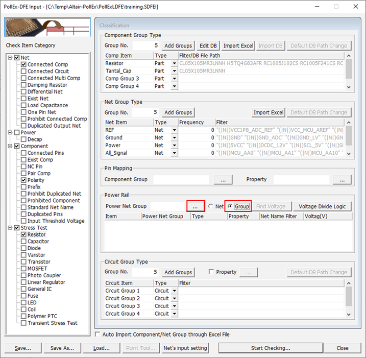
Setup Power Voltage Level.
In the Power Rail field, select Group in the
Power Rail section and click .
The Select Group dialog opens.Figure 52.
Enable the Power and
Ground checkboxes and click
OK.
Figure 53. The selected net groups are displayed in the Power Rail
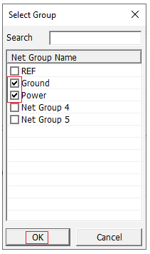
section.
For Ground, select Voltage(V).
This means that voltage will be assigned for all ground nets.
For Voltage (V), enter in 0.
Figure 54.
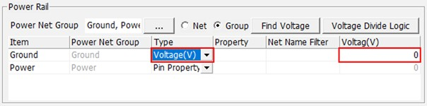
For Power, select Net Name.
For Net Name Filter, enter P.
This means that voltage value is included in net name string by the
rule of Number+P+Number.
Click Find Voltage to extract voltage value for
power and ground net.
All net names and voltages belonging to the Power and Ground net
groups are displayed in Power Rail section.Figure 55.
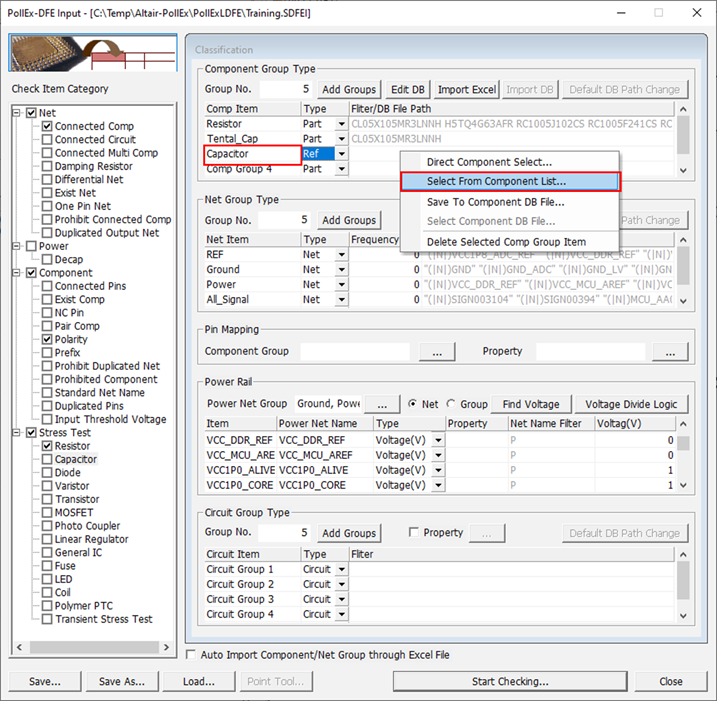
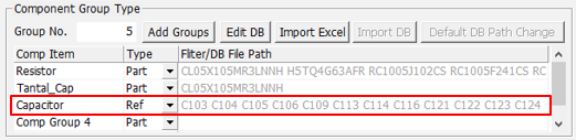
Define Capacitor component group.
In the Component Group Type section, click Component Group
3 and change the group name to
Capacitor by double-clicking the
name column.
For Capacitor, select Ref in the Type
column.
Right-click the same line and select Select from Component
List from the context menu.
Figure 56.
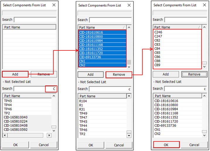
In the search field, enter C.
Click Add.
All components whole reference name begin with C will be
selected.
Select all components which reference names begin with CID- and CN and
click Remove to remove the selected components
from selected list.
Figure 57.
Click OK.
The selected list is registered as component group
Capacitor.Figure 58.
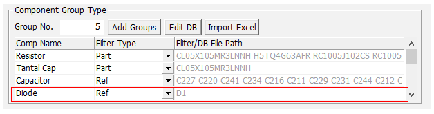
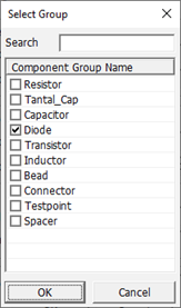
Define Diode component group.
In the Component Group Type section, click Component Group
4 and change the group name to
Diode.
For Diode, select Ref in the Type column.
Right-click the same line and select Selected Component from
List from the context menu.
In the search field, enter D at Search
field.
Select all components with reference names starting with CID- and click
Remove to remove the selected components from
the selected list.
Click OK.
The selected list is registered as the Diode component
group.Figure 59.
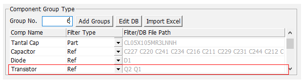
Define Transistor component group.
In the Component Group Type section, click Component Group
5 and change the group name to
Transistor.
For Transistor, select Ref in the Type
column.
Right-click the same line and select Select Component from
List from the context menu.
In the search field, enter Q and click
Add.
Click OK.
The selected list is registered as component group
Transistor.Figure 60.
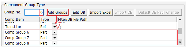
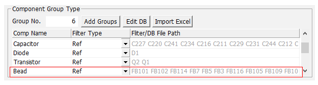
Define Bead component group.
In the Group No. field, enter 6 and click
Add Groups.
Figure 61.
In the Component Group Type section, click Component Group
6 and change the group name to
Bead.
For Bead, select Ref in the Type column.
Right-click the same line and select Selected Component from
List from the context menu.
In the search field, enter FB and click
Add.
Click OK.
The selected list is registered as component group Bead.Figure 62.
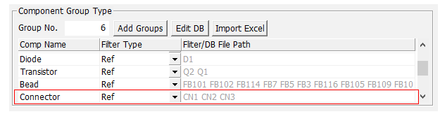
Define Connector component group.
In the Component Group Type section, click Component Group
7 and change the group name to
Connector.
For Connector, select Ref in the Type
column.
Right-click the same line and select Selected Component from
List from the context menu.
In the search field, enter CN and click
Add.
Click OK.
The selected list is registered as component group
Connector.Figure 63.
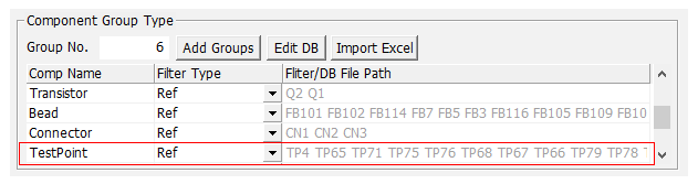
Define Testpoint component group.
In the Component Group Type section, click Component Group
8 and change the group name to
Testpoint.
For Testpoint, select Ref in the Type
column.
Right-click the same line and select Selected Component from
List from the context menu.
In the search field, enter TP and click
Add.
Click OK.
The selected list is registered as component group
Testpoint.Figure 64.
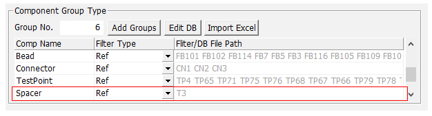
Define Spacer component group.
In the Component Group Type section, click Component Group
9 and change the group name to
Spacer.
For Spacer, select Ref in the Type column.
Right-click the same line and select Selected Component from
List from the context menu.
In the search field, enter T and click
Add.
Select all components with reference names starting with TP and TR and
click Remove.
Click OK.
The selected list is registered as component group Spacer.Figure 65.
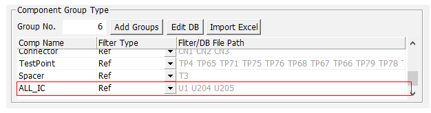
Define IC component group.
In the Component Group Type section, click Component Group
10 and change the group name to
All_IC.
For All_IC, select Ref in the Type column.
Right-click the same line and select Selected Component from
List from the context menu.
In the search field, enter U and click
Add.
Click OK.
The selected list is registered as component group All_IC.Figure 66.
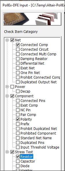
In the Check Item Category list, enable the Stress Test
and Resistor checkboxes.
Figure 67. The Stress Test/Resistor Item Rule Entry dialog
opens.
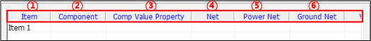
Set Stress Test/Resistor Item Test Condition
Figure 68.
Double-click the Component field to select a target
passive component to be tested.
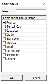
The Select Group dialog opens.Figure 69.
In the Select Group dialog, enable the
Resistor checkbox and click OK.
Double-click the Item field and enter
Resistor_Stress for the sub-item name.
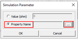
Double-click the Comp Value Property field.
The Simulation Parameter dialog opens. You can
assign a resistor value by entering resistor value or specifying the property
name where the resistor value is defined.Figure 70.
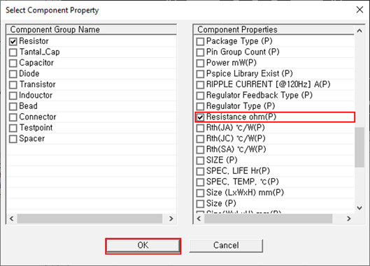
Select Property Name and click .
The Select Component Property dialog opens.Figure 71.
In the Component Group Name section, enable the Resistor
checkbox.
In the Component Properties section, enable the Resistance
ohm(P) checkbox.
Close the open dialogs.
Double-click the Net field to setup target net group to
which resistor is connected.
The Select Group dialog opens.
Enable the All-Signal checkbox and click
OK.
Figure 72.
Double-click the Power Net field to setup target power
net group to which resistor is connected.
The Select Group dialog opens.
Enable the Power checkbox and click OK.
Figure 73.
Double-click the Ground Net field to setup target ground
net group to which resistor is connected.
The Select Group dialog opens.
Enable the Ground checkbox and click OK.
Figure 74.
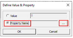
Double-click the Voh field.
The Define Value & Property dialog opens. You
can assign output high voltage level by entering Voh value or specifying the
property name where the Voh value is defined.Figure 75.
In the Define Value & Property dialog, select
Property Name and click .
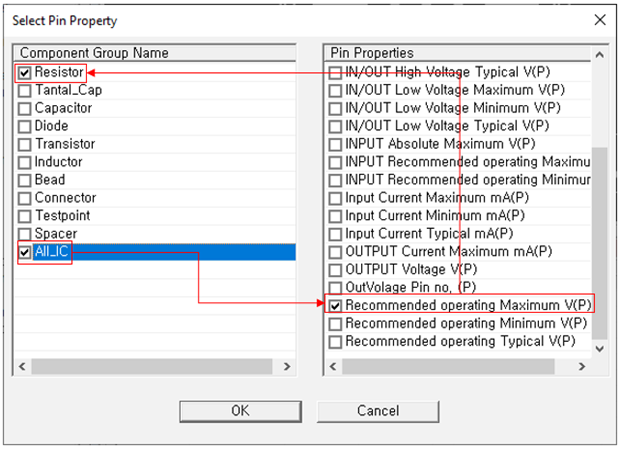
The Select Pin Property dialog opens.
In the Select Pin Property dialog, enable the
All_IC and Recommended operating Maximum
V(P) checkboxes.
When you select the property name, all components with the same property are
automatically selected. In this example, the resistor has a "Recommended
operating maximum" parameter, so it was selected at the same time.Figure 76.
Close the open dialogs.
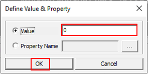
Double-click the Vol field.
The Define Value & Property dialog opens. You
can assign output low voltage level by entering Vol value or specifying the
property name where the Vol value is defined.Figure 77.
Select Value and enter 0.
Click OK to close the
Define Value & Property dialog.
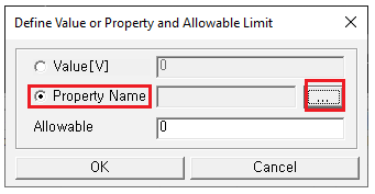
Enable the checkbox in the Working Voltage Check field and double-click the
Working Voltage Check field.
The Define Value or Property and Allowable Limit
dialog opens. You can assign maximum allowable rated Working Voltage level by
entering value or specifying the property name where the Working Voltage value
is defined.
Select Property Name option and click .
The Select Component Property dialog opens.Figure 78. Figure 79.
Enable the Resistor and MAX WORKING VOLTAGE
V(P) checkboxes and click OK.
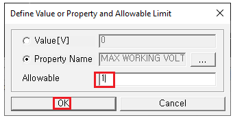
In the Define Value or Property and Allowable Limit
dialog, enter 1 for Allowable.
This means the allowable maximum working voltage is 1% of its rated Working
Voltage value.Figure 80.
Click OK.
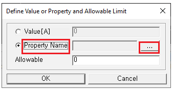
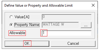
Enable the checkbox in the Power Dissipation Check field and double-click the
Power Dissipation Check field.
The Define Value or Property and Allowable Limit
dialog opens. You can assign maximum allowable rated Power Dissipation level by
entering value or specifying the property name where the Power Dissipation value
is defined.
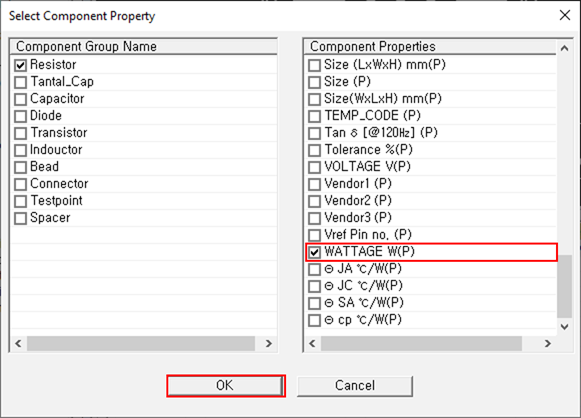
Select Property Name and click .
The Select Component Property dialog opens.Figure 81. Figure 82.
Enable the Resistor and WATTAGE
W(P) checkboxes and click OK.
For Allowable, enter 1.
This means the allowable maximum working voltage is 1% of its rated Power
Dissipation value.Figure 83.
Click OK.
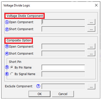
Enable the checkbox in the Stress Test Option field and double-click the
Stress Test Option field.
The Stress Test Option dialog opens. You can
specify the conditions to be used to search the voltage rail and signal net.
Upon double clicking this field.Figure 84.
In the Power Net Composite section, click for Open Component.
The Select Group dialog opens. You can assign
component group that will be considered as open state during searching voltage
rail.Figure 85.
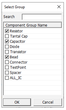
Enable the Resistor, Capacitor,
and Diode checkboxes and click OK.
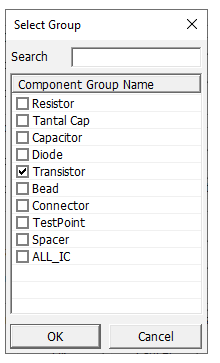
In the Power Net Composite section, click for Short Component.
The Select Group dialog opens. You can assign
component group that will be considered as short state during searching power
rail.Figure 86.
Enable the Transistor checkboxes and click
OK.
In the Signal Net Composite section, click for Open Component.
The Select Group dialog opens. You can assign
component group that will be considered as open state during searching signal
net.Figure 87.
Enable the Diode checkbox and click OK.
In the Signal Net Composite section, click for Short Component.
The Select Group dialog opens. You can assign
component group that will be considered as short state during searching signal
net.Figure 88.
Enable the Resistor, Capacitor,
and Bead checkboxes and click OK.
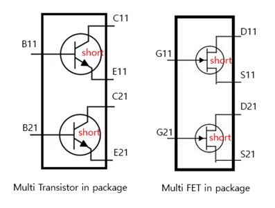
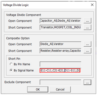
Select By Signal Name in the Short Pin section.
This means that we will define pin-connection information for multi-pin
component by signal name. For example, for the following multi-pin component,
the short pin pairs are C11-E11, C21-E21, D11-S11, and D21-S21.Figure 89.
For By Signal Name, enter E11-C11,
C21-E21, D11-S11,
D21-S21.
Figure 90.
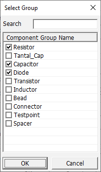
Click for Exclude Component.
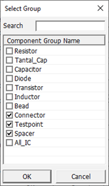
The Select Group dialog opens.Figure 91.
Enable the Connector, Testpoint,
and Spacer checkboxes and click OK.
Click OK to close the
Stress Test Option dialog.
Click Save to save current rule setup.
Run Stress Test/Resistor Item
In this step, you will run a stress test/resistor item and review the check
result.
Click Start Checking.
PollEx Logic DFE starts checking for selected
checking items. After running, PollEx Logic DFE changes
its window for results display.
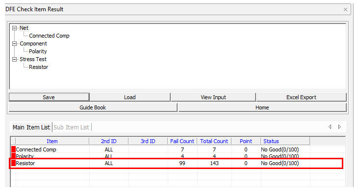
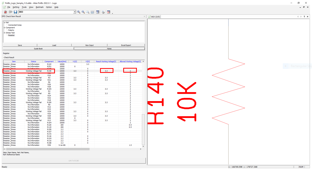
In the Result tab, click the Stress Test/Resistor item
to see the detailed result.
Figure 92.
To review the error, click on the error item marked R140
in the Component field of the Result tab.
In the right window, you can see the error location and a picture. Review the
list on the left and see the Working Voltage of R100 is 3.3V, but allowed
Working Voltage is 2.0V, so it fails.Figure 93.


 .
The Select Group dialog opens.
.
The Select Group dialog opens.