PollEx UPE (Unified Part Editor) is a software for managing
component 3D package geometry, footprint, logic symbol, signal integrity analysis
model, and thermal analysis information.
Create New Part Automatically
Click UPE in the PollEx Launcher.
The main window displays.
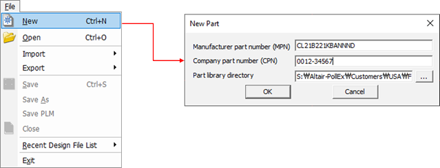
Create a new part.
From the menu bar, click File > New.
Enter CL21B221KBANNND for the Manufacturer part
number (MPN).
Enter 0012-34567 for the Company part number
(CPN) for the part.
Figure 1.
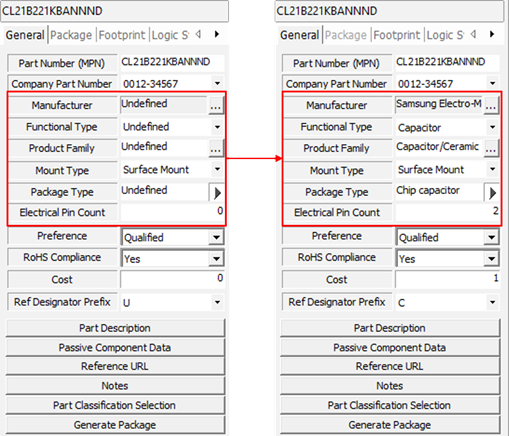
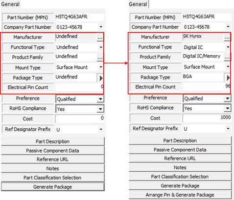
In the General tab, enter the component information.
Set Function Type to Capacitor.
Set Product Family to Capacitor/Ceramic.
Set Package Type to Chip Capacitor.
Set Electrical Pin Count to 2.
Function type, Product Family, Package Type, and Electrical Pint Count are
mandatory.Figure 2.
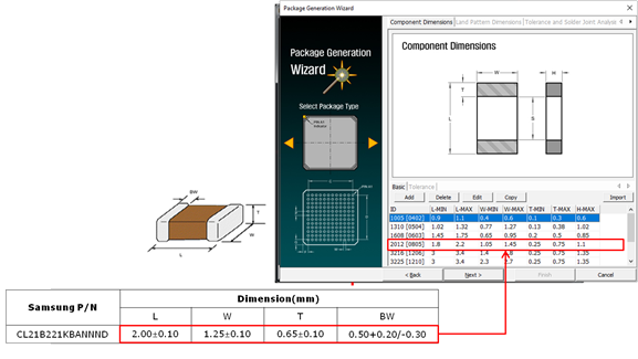
Generate a package using the package generation wizard.
Click Generate Package to open the Package
Generation Wizard and click Next.
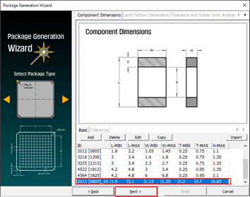
Refer to the component datasheet and select the item that matched the
size information of the component to be created.
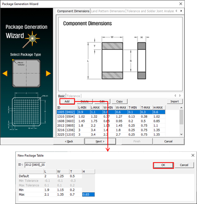
Figure 3. If no package in the package generation wizard matches with the
datasheet, create a new one by clicking Add and
specify each dimension of the component.Figure 4.
Select the item which dimension matches with the datasheet and click
Next.
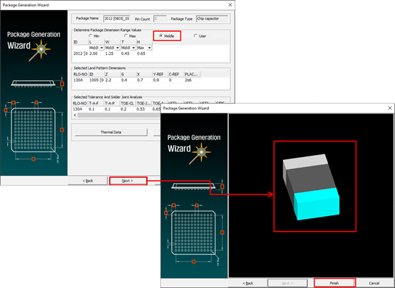
Figure 5.
Select Middle to specify all dimensions as
middle (typical) value and click Next.
The 3D package shape is created.Figure 6.
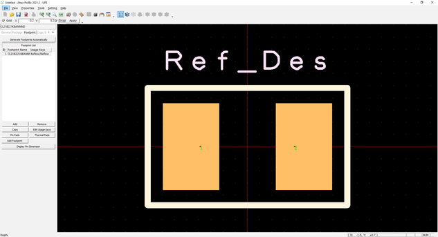
Generate a footprint automatically.
Click the Footprint tab.
Click Generate Footprint Automatically.
Figure 7. Then a footprint is generated based on the 3D component geometry.
The footprint is generated referring the footprint configuration table
editor.Figure 8.
Generate a footprint using footprint generation wizard.
This is useful when there is no configuration for the package in the footprint
configuration table, you cannot generate a footprint automatically.
Click Add.
Enter a name for the footprint generation and click Generate
Footprint.
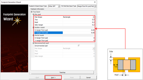
In the Footprint Generation Wizard window, enter the Pin pad, Solder
resist, and Metal mask information.
Click Next.
Figure 9.
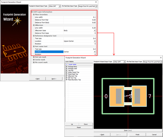
In the CAM Layer Information section, enter the Place boundary,
Silkscreen, Reference designator test, and Part name text information
and click Next.
The generated Footprint geometry can then be checked.Figure 10.
Generate a logic symbol automatically.
Click the Logic Symbol tab.
Click Generate Logic Symbol Automatically.
The Logic Symbol is generated.
Save the created part.
Click the General tab to check the general information
of the created part.
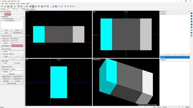
Check the package shape.
Click the Package tab.
Click Edit Package Body to check the shape of
the part.
Figure 11.
Click the Footprint tab to check the footprint shape of
the part.
Click the Logic Symbol tab to check the logic symbol
shape of the part.
Create New Part Manually
Create a new part.
From the menu bar, click File > New.
Enter H5TQ4G63AFR for the Manufacturer part
number (MPN).
Enter 0123-45678 for the Company part number
(CPN).
In the General tab, enter the component information.
For Package Type, select BGA.
For Electrical Pin Count, enter 96.
Package Type and Electrical Pin Count are mandatory.Figure 12.
Arrange pins and generate package.
Click Arrange Pin & Generate Package to open
the Package Generation Wizard.
Click Next.
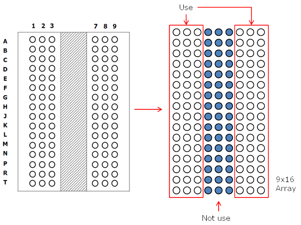
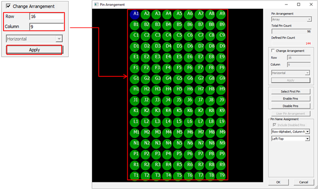
Set the pin arrangement as shown below and click
Apply.
Figure 13. Figure 14.
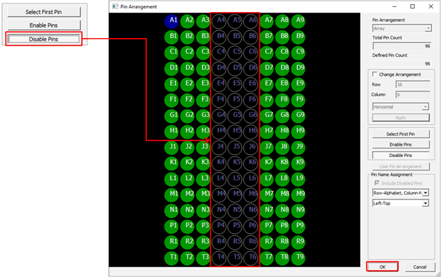
Click Disable Pins and select the pins that are
not used.
Click OK.
Figure 15.
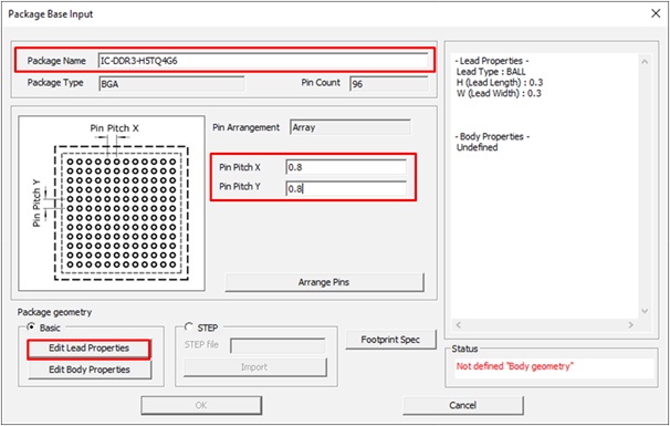
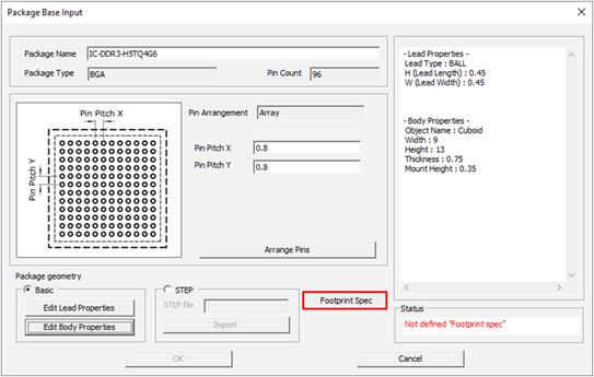
Define the package name and pin pitches.
Click Edit Lead Properties to define the lead
pin properties.
Figure 16.
In the Package Lead Editor, define the lead type as BALL, specify the
size, and click OK.
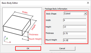
Click Edit Body Properties.
In the Basic Body Editor dialog, select the body
shape and input the body size by referring to the datasheet.
Click OK.
Figure 17.
Click Footprint Spec to define the footprint
specifications.
Figure 18.
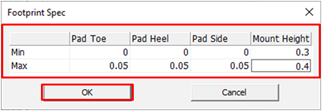
Enter the toe, heel, and side size of the pin pad and mount height of
the body and click OK.
Figure 19. Now all items in the package base are defined.
Click OK.
The created package displays in the package tab window.
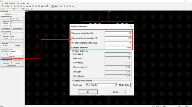
From the menu bar, click Package > Thermal in the Package tab to add package thermal characteristic
properties.
In the Package Thermal dialog, enter the thermal
characteristics of the package.
Figure 20.
Click OK to save the
part data.
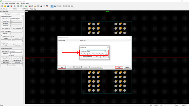
Click Add to add a simulation library for signal
integrity analysis.
In the device model files dialog, click Add and
select the model library type and file:
C:\ProgramData\altair\PollEx\<version>\Examples\UPE\ddr3_4g_x16.ibs.
Figure 21.
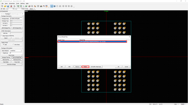
Click OK to add the
device model file.
Select the device model file and click
Display.
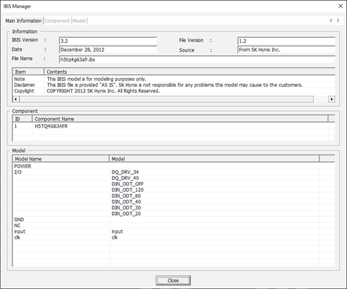
Figure 22. You can see the detailed information of the device model file.Figure 23.
Click Close to close the device model
information and click OK to close the device model file setting.
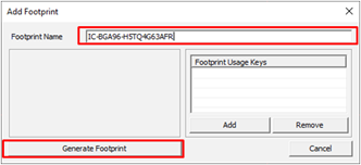
Generat a footprint.
Click the Footprint tab and click
Add.
Enter a name for the footprint generation and click Generate
Footprint.
Figure 24.
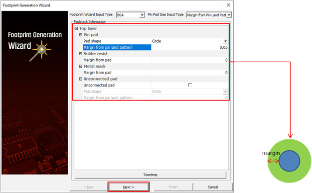
In the Footprint Generation Wizard, enter the Pin pad, Solder resist,
and Metal mask information and click Next.
Figure 25.
In the CAM Layer Information section, enter Place boundary, Silkscreen,
Reference designator test, and Part name text information.
Click Next.
The generated Footprint geometry can be checked.
Click Finish.
Generate a logic symbol.
Click the Logic Symbol tab and click
Add to add a logic symbol.
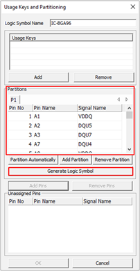
Enter a name for logic symbol, select all pins in the unassigned pins
area, and click Add Pins.
In the Add Partition dialog, enter a partition
name and click OK.
The selected pins are moved to the partitions area.
Click Generate Logic Symbol to generate a logic
symbol.
Figure 26.
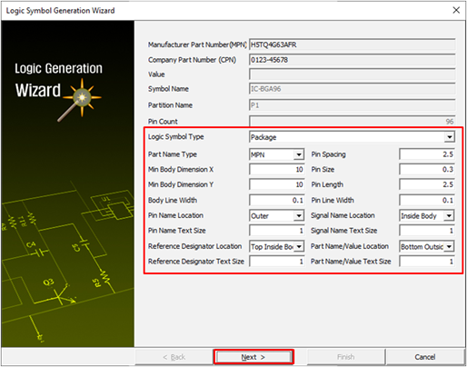
In the logic symbol generation wizard, enter the dimension size of pins
and body and define the locations where part properties are
placed.
Figure 27.
Click Next.
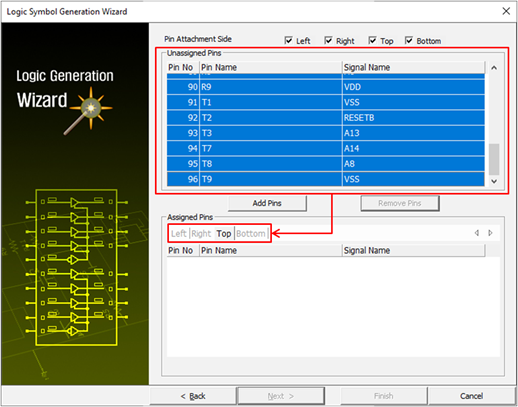
Place pins to all directions of the body.
Twenty-four pins will be placed to each side. One to 24 at left side,
25 to 48 at bottom side, 49 to 72 at right side and 73 to 96 at top
side.Figure 28.
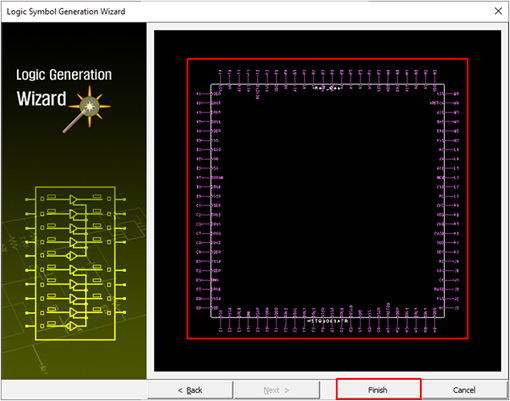
Click Next to confirm the logic symbol.
Confirm the created logic symbol and click
Finish to close the logic symbol generation
wizard.
Figure 29.
Click the General tab to check the general information
of the part.
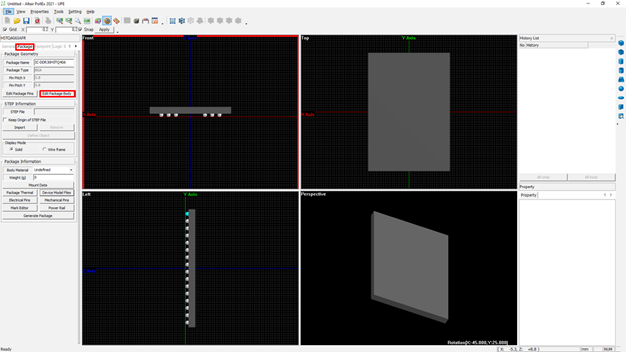
Click the Package tab and click Edit Package
Body to check the package shape of the part.
Figure 30.
Click the Footprint tab to check the footprint shape of
the part.
Click the Logic Symbol tab to check the logic symbol
shape of the part.